On these pages, I will explain the hardware specification of PICF873. The contents of the explanation is the part which is different from PIC16F84A. So, as for the basic specification, refer to PIC16F84A. As for the detail specification, refer to PIC16F873.
PIC16F873 is PIC which has a lot of feature than PIC16F84A. The program memory is 4K Words, the RAM memory is 192 bytes and the EEPROM is 128 bytes. It has three kinds of timers, Analog Digital converter, Universal communication port....
Flash memory is used for PIC16F873 like PIC16F84A. So, the program can be easily rewritten by the PIC programmer. This is very convenient.
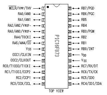
| RA0-5 : | Input/Output port A |
| RB0-7 : | Input/Output port B |
| RC0-7 : | Input/Output port C |
| AN0-7 : | Analog input port |
| RX : | USART Asynchronous Receive |
| TX : | USART Asynchronous Transmit |
| SCK : | Synchronous serial clock input |
| SCL : | Output for both SPI and I2C modes |
| DT : | Synchronous Data |
| CK : | Synchronous Clock |
| SDO : | SPI Data Out ( SPI mode ) |
| SDI : | SPI Data In ( SPI mode ) |
| SDA : | Data I/O ( I2C mode ) |
| CCP1,2 : | Capture In/Compare Out/PWM Out |
| OSC1/CLKIN : | Oscillator In/Ecternal Clock In |
| OSC2/CLKOUT : | Oscillator Out/Clock Out |
|
| MCLR : | Master Clear ( Active low Reset ) |
| Vpp : | Programming voltage input |
| THV : | High voltage test mode control |
| VREF+/- : | Reference voltage |
| SS : | Slave select for the synchronous serial port |
| T0CKI : | Clock input to Timer0 |
| T1OSO : | Timer1 oscillator output |
| T1OSI : | Timer1 oscillator input |
| T1CKI : | Clock input to Timer1 |
| PGD : | Serial programming data |
| PGC : | Serial programming clock |
| PGM : | Low voltage programinng input |
| INT : | External interrupt |
| VDD : | Positive supply for logic and I/O pins |
| Vss : | Ground reference for logic and I/O pins |
|
|