|
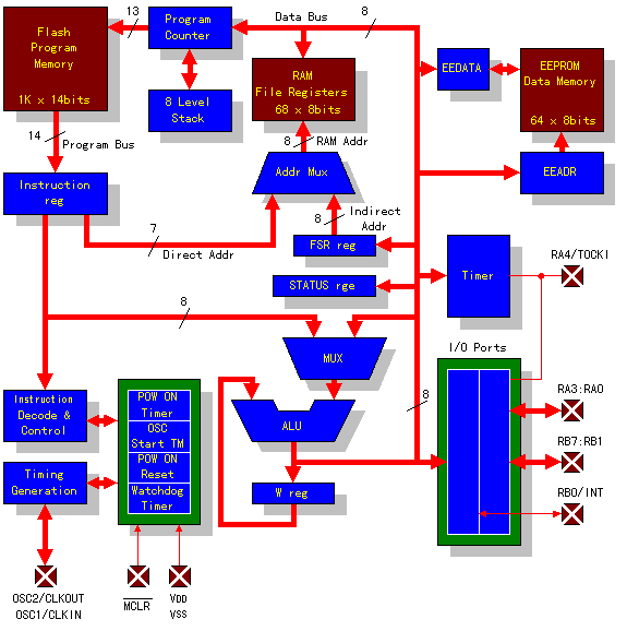
 Flash Program Memory Flash Program Memory |
|
Flash memory is used to store the program. One word is 14 bits long and 1024 words (1k words ) can be stored. Even if power is switched off the contents of the flash memory will not be lost. Flash memory can be written to using the writer, but the number of times it be rewritten is limited to 1000 times.
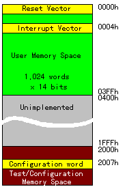 | The usage of some program memory addresses is already decided. |
|
 Reset Vector ( 0000h ) Reset Vector ( 0000h ) |
| When a reset is executed, either by turning power on, by the WDT (Watchdog Timer) or any other factor, the program will start from this address. |
|
| Peripheral Interrupt Vector ( 0004h ) |
| When there is a time-out interruption from the timer (TMR0) or an outside interrupt, the program will start from this address. |
|
| Configuration word ( 2007h ) |
|
The basic operation of the PIC is specified at this memory location. The enable bits of the Power-up timer, and the Watch-dog timer as well as the oscillator selection bits are set here.
This area is behind the usual program area and can not be accessed by the program. These parameters must be specified using the burner when burning the program into flash memory.
For details about the configuration word refer to "Detailed specifications of the PIC16F84A(1)". |
|
|
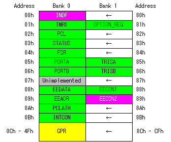
| RAM(Random Access Memory) File Registers |
|
Bank switching is used to access this memory. Each bank has a memory capacity of 80 bytes (00h-4Fh). The PIC16F84A has two banks.
This memory is divided into two sections.
The first 12 bytes (00h-0Bh) of each bank are called SFR (Special Function Registers) and are used to record the operating states of the PIC, the input/output (I/O) port conditions and other conditions.
There are 16 different registers in the SFR (11 in bank 0 and 5 in bank1). The content of each register is managed by the PIC. Although there are a total of 24 file registers, several of them are in both banks.
The remaining 68 bytes (0Ch-4Fh), from byte 13 upward, are called GPR (General Purpose Registers) and can be used to temporally store results and conditions while the program is running.
The contents of the GPR are the same in both banks, so even with bank switching the total capacity is only 68 bytes.
The contents of the GPR are lost when the power is switched off. There is no limit to the number of times data can be rewritten. |
|
| EEPROM(Electrically Erasable Programmable Read Only Memory) |
|
This is nonvolatile memory, the contents is not lost when power is turned off. The memory contents can be rewritten by the program. The total capacity is 64 bytes, and the number of times it can be rewritten to is limited to about one million. For this reason it is not recommended for temporary data storage. It is used to store data which will not change frequently.
Data can be safely stored for 40 years. |
|
| SFR Registers |
|
16 different SFR (Special Function Registers) can be specified by the bank switching technique. The figure below shows the RAM File Registers. The memory capacity is only 160 bytes. The contents of the registers with the left pointing arrow are the same on both banks. The other registers of the SFR are accessible through bank switching, and the gray colored registers are not used.
For details about each register refer to "Detailed specifications of the PIC16F84A(1)". |
|
| Program Counter |
| This counter contains the address of the next instruction ( fetch address) to be read from the program memory (flash memory). It is a 13 bit counter. Generally the count increments each time an instruction is executed, and the location of the following instruction is shown in the PC. But when a jump is executed the contents of this counter is rewritten to that of the jump address. |
|
| 8 Level Stack |
|
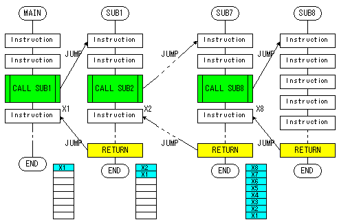
The stack stores the program return address when a jump is executed.
For example if the same instructions are to be executed more than once, a subroutine is used. A RETURN instruction signifies the end of the subroutine and the program continues were it left off. A CALL instruction tells the program to jump to a subroutine. When the CALL instruction is encountered, the return address (the address of the instruction immediately after the CALL) is stored at the top of the stack. This operation is sometimes called a PUSH. When the subroutine processing is finished and the RETURN instruction is executed, the address at the top of the stack is put in the PC and the program continues normal execution. This operation is sometimes called a POP. This way multiple subroutines can be called and the processing will return to the part of the program which called the subroutine.
Since there are eight stack registers, eight subroutine calls can be made sequentially. After the eighth, a call will roll the contents of the eighth (and last register) back to the top of the stack. When a return is executed, the PC will send the program to the wrong address, and the program will not work properly. For this reason only eight sequential subroutines calls can be made.
A return from a subroutine call must be done by the RETURN instruction. Never use the JUMP instruction to return from a subroutine.
|
|
| Instruction Register |
| The instruction at the address specified by the PC is read to this register. This operation is called a FETCH. |
|
| Instruction Decode & Control |
| The instruction in the Instruction Register is analyzed here, and (according to its contents) the operation is performed. |
|
| Multiplexer and Arithmetic Logic Unit |
| The calculations are performed by the Multiplexer and Arithmetic Logic Unit (ALU).Without these two it would not be a computer. |
|
| W Register |
| This is the working register. It is used to temporarily store the contents of the ALU. It is indispensable for calculation operations. The contents of this register can be transferred to the various registers to be utilized by the program. It is also used to control the I/O ports. |
|
| STATUS Register |
|
This Register stores the result of the ALU (Zero, positive or negative), a time-out condition, register bank select etc.
For details on the Status Register refer to "Detailed specifications of the PIC16F84A(1)". |
|
| FSR Register |
|
FSR (File Select Register) is used to specify the address of the RAM file register when using the indirect addressing method.
In the direct address method the register address is specified by the program instructions. In this case a 7 bit address, from 0 to 127, can be specified. This range is for one bank. To change the bank, the RP0 bit of the status register must also be specified. Since the FSR is 8 bits, it is possible to specify the address and bank at the same time, saving instruction cycles. In the PIC16F84A memory locations 80 (50h) to 127 (7Fh) are not installed.
When using the FSR it is convenient to make the file register data area continuous. Incrementing the FSR simplifies processing during read and write operations. |
|
| Address Multiplexer |
| Distinguishes between direct and indirect addressing. |
|
| EEDATA |
| This register is used when reading from, or writing data to the EEPROM. |
|
| EEADR |
|
This register specifies the EEPROM address. Since it is composed of eight bits addresses from 0 to 255 can be specified. The PIC16F84A has only 64 bytes of memory installed. The address of EEPROM is started from 2100h.
When writing data during program execution it is necessary to sequentially write 55h then AAh to the EECON2 register. |
|
| Timer |
|
The PIC16F84A has only one timer (TMR0, an 8 bit timer). It times out when the count reaches 256 and the TOIF bit of the INCON register of the SFR becomes "1". With a timed out condition it is possible to make an interrupt occur. The interrupt will stop the processing which was in progress at that time. To make the interrupt occur the GIF and the TOIE bits of the INTCON register of the SFR must be set (1)
For details of the timer refer to "Detailed specifications of the PIC16F84A(3)". |
|
| I/O Ports |
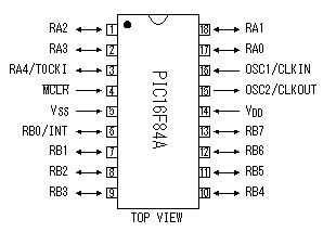
| There are 13 I/O pins, with individual direction controls. The mode (input or output) of each pin can be set from within the program. The 13 pins are divided into two groups. The A Port has five pins and the B Port has eight. There is a limitation on control timing, but each of the 13 pins can be individually controlled. For details of the I/O Ports refer to "Detailed specifications of the PIC16F84A(2)". |
|
| Timing Generation |
|
This circuit generates the clock pulses which determine the speed of operation. Oscillator operation is determined by external capacitors and a crystal (or ceramic) oscillator. If high stability is desired a crystal or ceramic resonator is used. Generally the circuitry is simpler with the resonator, which incorporates the ceramic and capacitors in one module. An external clock can also be used.
The PIC16F84A executes one instruction (one cycle) every four clock pulses, using pipeline architecture. But when a JUMP is executed two cycles are necessary (8 clock pulses). With a 20MHz clock the execution time of an instruction is 200ns. (The pulse period of 20MHz is 50ns (1 / 20MHz = 50ns), so 50ns x 4 cycles = 200ns). 5,000,000 instructions can be executed in one second. (2,000,000 / 4 = 5,000,000) |
|
| Initialization circuits |
|
The PIC16F84A has various initialization circuits.
| POW ON Timer | : | When power is turned on this timer inhibits operation until the voltage is stable. |
| OSC StartTimer | : | When power is turned on this timer inhibits operation until the clock is stable. |
| POW ON Reset | : | When power is turned on this timer initializes the inner circuitry of the PIC. |
Watchdog Timer

| : | This timer watches over the normal operation of the PIC software. It must be regularly cleared by software. When it times out the PIC returns to the point in the program immediately after power on. This timer is used to recover program operation when the software has a defect (or bug). Even if the program is reinitialized the bug is still in the program. |
|