|
On this page, I will explain the programming specification( ICSP : In-Circuit Serial Programming ) of the PIC16F84A.
A PIC programmer is used for the programming the PIC.
Since the PIC programmer automatically controls the ICSP, you don't need to know this specification to program a PIC.
I intend to make a programmer in the near future, and examined the specification in order to understand how it works.

 Specification of ICSP Specification of ICSP
The PIC16F84A program is written into flash memory. In order to program the flash memory the following specification is used.
The following five pins are used for reading and writing the data. |
| Pin Name | Pin No. | During Programming |
| Pin Name | Pin Type | Pin Description |
| RB6 | 12 | CLOCK | I | Clock input |
| RB7 | 13 | DATA | I/O | Data input/output |
| MCLR | 4 | VTEST MODE | P | Program Mode Select |
| VDD | 14 | VDD | P | Power Supply |
| VSS | 5 | VSS | P | Ground |
|
I = Input,O = Output,P = Power
To activate the programming mode, high voltage( VHH = +13V ) must be applied to the MCLR input.
Also, +5V is applied to VDD. |
Programming is done by the following procedure. First +5V must be applied to VDD.
 Program/Verify Mode Program/Verify Mode
 | (1) RB6, RB7 and MCLR are made 0V (Low). |
| (2) Raise MCLR pin from 0V(Low) to +13V(VHH). |
| The PIC is now in Program/Verify mode. |
Serial Program/Verify Operation
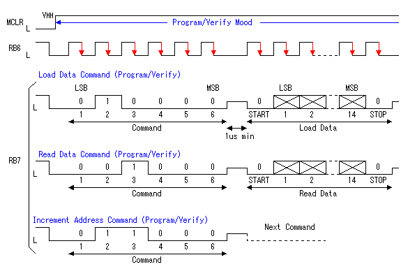
| Pin RB6 is used as a clock input pin, and the RB7 pin is used for entering command bits and for data input/output during serial operation. |
| Writing or reading of data is done using the above two pins. |
When using the PIC in Program/Verify mode, the internal clock is not used. Data input/output is controlled by the RB6 clock input.
When the PIC is mounted on an application PCB and the clock cannot be disabled, upon the application of power MCLR must be taken to VHH before the PIC begins operation (About 72 milliseconds).
Otherwise, if the PIC begins operation the program counter will be incremented and the writing start address will be offset.
When using a programmer this problem will not be encountered, since the internal clock generator is not used.
Detail specification of Program/Verify mode
About serial method
RB6 (Clock input) and RB7 (Data input/output) are used for reading and writing of data to or from the PIC. The data is transmitted or received serially. RB7 data consists of a 6-bit command and 16 data bits.
The 16 data bits are made up of one start bit, 8 bits (one byte) of data memory and one stop bit. The remaining 6 bits are ignored.
All commands and data words are transmitted least significant bit(LSB) first.
Each command and data bit is latched on the falling edge of the RB6 clock pulse. During a read operation the LSB will be transferred to the RB7 pin on the rising edge of the second cycle of the RB6 clock pulse.
Command Mapping
The following nine commands to use in Program/Verify mode.
| Command |
Mapping
 | Data |
| Load Configuration |  | 0, data( 14 ), 0 |
| Load Data for Program Memory |  | 0, data( 14 ), 0 |
| Read Data from Program Memory |  | 0, data( 14 ), 0 |
| Increment Address |  | None |
| Begin Programming |  | None |
| Load Data for Data Memory |  | 0, data( 14 ), 0 |
| Read Data from Data Memory |  | 0, data( 14 ), 0 |
| Bulk Erase Program Memory |  | None |
| Bulk Erase Data Memory |  | None |
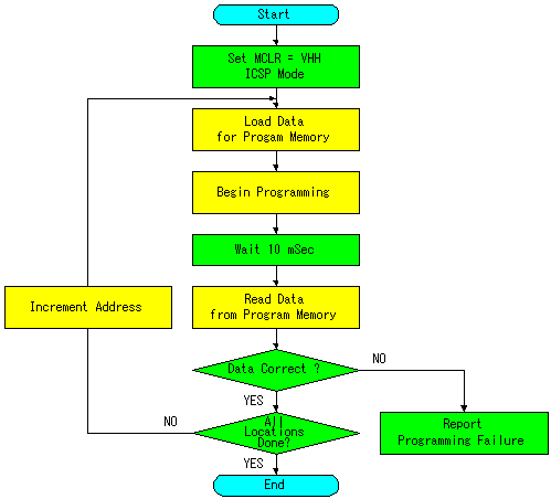
Program flow chart
Below is a programming flow chart of program memory in Program/Verify mode.
Below is a programming flow chart of configuration data in Program/Verify mode.
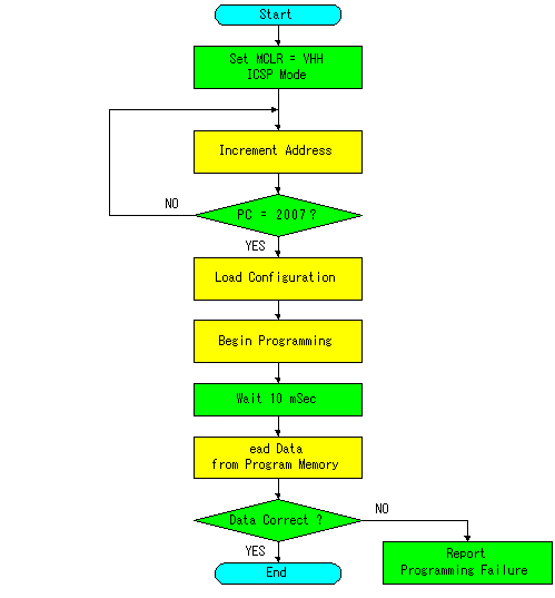
Once in configuration memory(PC >= 2000h), the highest bit(14th bit) of the PC stays a '1', thus always pointing to the configuration memory. The only way to point to user program memory is to reset the part and reenter program/verify mode.
Microchip Inc. recommends that VDD be made minimum voltage and then maximum voltage after the above-mentioned processing and then read the data to verify it is correct. |
|