I/O Port of PIC16F873
|
On this page, I will explain about Input/Output port of PIC16F873.
There are 22 ports in total. 6 ports as Port A, 8 ports as Port B, 8 ports as Port C. When using as the input/output port of the digital signal, the A port, the B port and the C port can be similarly used. However, some ports are used also as the other feature port in addition to the digital signal I/O port. Port A is composed of 6 ports to RA5 from RA0. These ports can also be served as the input port of the analog signal, the input port of analog reference voltage, the input port of the timer0 clock of the outside so on. 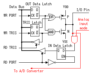 The circuit is the same as PIC16F84A approximately but a selecting circuit for the analog input is incorporated. The circuit is the same as PIC16F84A approximately but a selecting circuit for the analog input is incorporated.When using for the digital signal I/O port, input mode or output mode are specified by the TRISA register. In case of not being the digital signal I/O port, the feature of each port is specified by ADCON0 and ADCON1 registers. When setting analog signal input, the specification of the TRISA register is effective. So, when using as the analog signal input port, the corresponding bit of TRISA register must be set to input mode "1". Port B is composed of 8 ports to RB7 from RB0. These ports can also be served as the programming port in addition to the digital signal I/O port. There is not a setting register when using as the programming port. It is automatically used as the programming ports by the ICSP programming. As for ICSP, refer to the item of PIC16F84A. 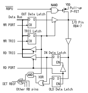 Four of port B, RB7 to RB4, have an interrupt on change feature. When the circuit detects the change, RBIF bit of INTCON register will be set and program conter will be change to address 4( Interrupt Vector ). Four of port B, RB7 to RB4, have an interrupt on change feature. When the circuit detects the change, RBIF bit of INTCON register will be set and program conter will be change to address 4( Interrupt Vector ).The RB0/INT port can be used as an external interrupt input pin. When using this feature, the INTE bit of the INTCON register should be set to "1" and rising detection(1) or falling detection(0) should be selected by the INTEDG bit of the OPTION_REG register. Also, port B has a pull-up feature. This feature is the feature to make the condition of the port H level condition when nothing is connected with the port. Eight all of the ports become a pull-up condition by making the RBPU bit of OPTION_REG "0". This feature is effective only in the input mode. When set to the output mode with the TRISB register, the port is detached from the pull-up circuit. The circuit is same as PIC16F84A. Port C is composed of 8 ports to RC7 from RC0. These ports can also be served as the clock input port of the Timer0, the ports for the various communication so on. 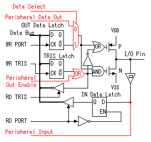 RC0 can also be served as the connection port of the oscillator for timer1 or the clock input port of timer1. It is possible to select the feature by setting of T1CON register. RC0 can also be served as the connection port of the oscillator for timer1 or the clock input port of timer1. It is possible to select the feature by setting of T1CON register.RC1 can also be served as the connection port of the oscillator for timer1 or the CCP2(Capture2 input/Compare2 output/Pulse Width Modulation2(PWM2) output) port. It is possible to select the feature by the setting of T1CON register about Timer1. Also, it is possible to select the feature by the setting of CCP2CON register about CCP2. RC2 can also be served as the CCP1 port. When using as the port of CCP1, it is possible to select the feature by the setting of CCP1CON register. RC3 can also be served as the clock input port of the synchronous serial communication or the output port of the SPI(Serial Peripheral Interface)/I2C(Inter-Integrated Circuit). RC4 can also be served as the SPI data input port or the data input/output port by the I2C mode. RC5 can also be served as the SPI data output port. To use the SPI/I2C mode, INTCON/PIR1/PIE1/SSPBUF/SSPCON/SSPSTAT registers should be set. RC6 can also be served as the USART(Universal Synchronous Asynchronous Receiver Transmitter) asynchronous transmission port or the clock port of the synchronous communication. RC7 can also be served as the asynchronous receiving port by the USART or the data port of the synchronous communications. To use USART communication or synchronous communication, TXSTA/TXREG/RCSTA/RCREG/SPBRG/PIR1/PIE1 registers should be set. The figure is the circuit diagram of RC0-2 and RC5-7. In case of RC3 and RC4, a selecting circuit for SSPI is added to the input circuit. |