The function of A/D converter is to change the measurement result of the voltage of the analog input signal into the digital information.
PIC16F873 changes into the 10-bit digital information. So, the measurement result can be displayed in the precision of 1/1024 in the maximum range. It is possible to measure in the about 5mV precision (5/1024=0.004883), supposing that the maximum measuring range is 5V(From 0V to +5V).
 Input port Input port
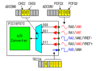
In PIC16F873, a maximum of 5 ports can be specified as the analog input port. Because the A/D conversion module is one, so, it can do only the measurement of 1 port at the same time. If measuring each port in the order, more than one port can be measured. Because the measuring time is an about 40-u seconds, the changing analog voltage can be measured. It isn't possible to do the measurement of the high frequency.
PCFG
3210 | Port | Remarks |
| AN4 | AN3 | AN2 | AN1 | AN0 |
| 0000 | A | A | A | A | A |
|
| 0001 | A | VREF+ | A | A | A |
|
| 0010 | A | A | A | A | A | Same as 0000 |
| 0011 | A | VREF+ | A | A | A | Same as 0001 |
| 0100 | D | A | D | A | A |
|
| 0101 | D | VREF+ | D | A | A |
|
| 0110 | D | D | D | D | D |
|
| 0111 | D | D | D | D | D | Same as 0110 |
| 1000 | A | VREF+ | VREF- | A | A |
|
| 1001 | A | A | A | A | A | Same as 0000 |
| 1010 | A | VREF+ | A | A | A | Same as 0001 |
| 1011 | A | VREF+ | VREF- | A | A | Same as 1000 |
| 1100 | A | VREF+ | VREF- | A | A | Same as 1000 |
| 1101 | D | VREF+ | VREF- | A | A |
|
| 1110 | D | D | D | D | A |
|
| 1111 | D | VREF+ | VREF- | D | A |
|
|
The input analog port is designated by PCFG3-0 bits of ADCON1 register. The patterns which can be designated by these 4 bits are beforehand decided.
The port which connects with the A/D conversion module is designated by CHS0, CHS1 and CHS2 of the ADCON0 register. The analog input port should be set as input mode with setting the corresponding bit of TRISA register.
There are the same patterns more than one. It is because the pattern is shared in the PIC16F87x series.
A: Analog port
D: Digital port
VREF+: High reference voltage
VREF-: Low reference voltage
|
Measurement range and measurement precision
As for the measurement range, the range of VDD(+5V) from VSS(0V) is basic range. Besides, it is possible to set in VREF-(Low reference voltage) and VREF+(High reference voltage). But, VREF- and VREF+ must be the inside of the range of VDD from VSS.
For example, if it makes the side of the low voltage to VSS(0V) and the side of the high voltage to 3V by VREF+, then the measuring range becomes 3V. Because this range is measured in the precision of 1/1024, the measurement precision in this case is 3/1024=0.002929 (about 3mV).
 |
The use of VREF- or VREF+ can be designated by the pattern of PCFG0-3 of the ADCON1 register.
When VREF- and VREF+ are specified, the difference voltage which is inputted on AN2 and AN3 is a measuring range.
When only VREF+ is specified, the low voltage is VSS.
When VREF- and VREF+ aren't specified, the low voltage is VSS and the high voltage is VDD. |
Result of A/D conversion
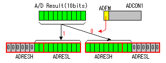 | The ADRESH and ADRESL register pair is the location where the 10 bits A/D result is loaded at the completion of the A/D conversion. This register pair is 16 bits wide. The A/D module gives the flexibility to left or right justify the 10 bits result in the 10 bits result register. The A/D Format Select bit (ADFM) of ADCON1 register controls this justification. The extra bits are loaded with 0. |
Mechanism of the measurement of the analog voltage
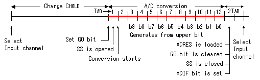
The sample/hold capacitor (CHOLD) in A/D converter module is charged by the voltage applied from analog input port. The voltage of CHOLD is converted to the digital value with A/D converter. So, it is necessary to wait until the CHOLD is charged fully after selecting the input analog channel by setting CHS0-3 of ADCON0 register. This time isn't automatically secured. The start timing of A/D converter after selecting the input channel must be controlled by software. It needs about 20u seconds to start A/D converter after setting input channel.
The shortest A/D conversion time is an about 20u seconds. It depends on the conversion clock. During this time, the CHOLD is disconnected from analog input.
A/D conversion starts when GO bit of ADCON0 register is set. When the A/D conversion is complete, GO bit will be cleared by hardware. There are two way to detect the completion of A/D conversion. One is the way of polling for the GO bit to be cleared. One more way is the way which use interruption. In case of the interruption, ADIE bit of PIE register and GIE bit of INTCON register should be set. When the conversion is complete, ADIF bit of PIR1 register is set and interruption occurs.
 |
The circuit block which CHOLD charges by the analog input voltage is shown in the left figure. CHOLD is charged when sample switch (SS) is closed. The diode is for the protection when voltage over VDD or voltage under the grounding is applied to the input.
| CHOLD: | Sample/Hold capacitance ( 120pF ) |
| RSS: | Sampling switch resistance( about 7K-ohm at VDD=5V ) |
| SS: | Sampling switch |
| RIC: | Interconnect resistance ( =<1K-ohm ) |
| CPIN: | Input capacitance ( 5pF ) |
| ANx: | Input pin |
| RS: | Analog source impedance ( =<10K-ohm ) |
| VA: | Analog source voltage |
|
A/D conversion clock
| Device clock | Operation | ADCS1 | ADCS0 | Calculation |
| Less 1.25MHz | Fosc/2 | 0 | 0 | (1/1.25)*2=1.6 uS |
| Less 5MHz | Fosc/8 | 0 | 1 | (1/5)*8 =1.6 uS |
| Less 20MHz | Fosc/32 | 1 | 0 | (1/20)*32=1.6 uS |
| Inner RC | RC | 1 | 1 | About 4 uS |
RC is used when doing A/D conversion under SLEEP mode. |
A/D conversion is executed based on the A/D conversion clock. For correct A/D conversions, the A/D conversion clock(TAD) must be selected to ensure a minimum TAD time of 1.6u seconds.
One conversion clock from four kinds of clock patterns can be selected by ADCS0 and ADCS1 bits of ADCON0 register.
The resultant TAD times deriver from the device operating frequencies and the A/D clock source selected is shown below. |
In PIC16F873, the A/D conversion takes 12-bit time. Actually, the conversion is 10 bits but more 2 bits (pre-processing time and post-processing time) is necessary. When supposing that the conversion time of 1 bit is 1.6 uS, the total conversion time is 1.6 x 12 = 19.2u seconds.
In case of the 10MHz clock, Fosc/32 is chosen. In this case, the conversion time of 1 bit is (1/10) x 32=3.2 uS and it takes 38.4u seconds for 12 bits.
Software processing of the A/D converter
 When not using interruption processing When not using interruption processing
| 1. Configure the A/D module ( Initialization process ) |
 | Configure analog pins/voltage reference/and digital I/O | ADCON1/PCFG0-3 |
| Select A/D conversion clock | ADCON0/ADCS0-1 |
| Turn on A/D module | ADCON0/ADON |
 |
| 2. Configure input channel |
| Select A/D input channel | ADCON0/CHS0-2 |
|
| 3. Securing of the condenser charging time |
| Wait until the CHOLD is charged fully | About 20u seconds |
|
| 4. Start conversion |
| Set GO bit | ADCON0/GO=1 |
|
| 5. Wait for A/D conversion to complete |
| Polling for the GO bit to be cleared | ADCON0/GO=0? |
|
| 6. Read A/D result register pair |
| Read A/D result register pair | ADRESH,ADRESL |
|
| 7. For next conversion, go to step 1 or 2 as required. |
|
When using interruption processing
| 1. Configure the A/D module ( Initialization process ) |
| Configure analog pins/voltage reference/and digital I/O | ADCON1/PCFG0-3 |
| Select A/D conversion clock | ADCON0/ADCS0-1 |
| Turn on A/D module | ADCON0/ADON |
|
| 2. Configure input channel |
| Select A/D input channel | ADCON0/CHS0-2 |
|
| 3. Set the condition of interruption |
| Clear ADIF bit | PIR1/ADIF=0 |
| Set ADIE bit | PIE/ADIE=1 |
| Set GIE bit | INTCON/GIE=1 |
|
| 4. Securing of the condenser charging time |
| Wait until the CHOLD is charged fully | About 20u seconds |
|
| 5. Start conversion |
| Set GO bit | ADCON0/GO=1 |
|
| 6. Wait for A/D conversion to complete |
| Waiting for the A/D interrupt |
|
|
| 7. Read A/D result register pair |
| Read A/D result register pair | ADRESH,ADRESL |
| Clear ADOF bit | PIR1/ADIF=0 |
|
| 8. For next conversion, go to step 1 or 2 as required. |
|
In case of the interruption way, the feature share of main process and interruption process must be examined.
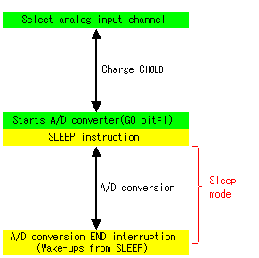
A/D operation during sleep
The A/D module can operate during sleep mode to eliminate all digital switching noise from the conversion.
For the A/D module to operate in sleep, the A/D clock source must be set to RC by setting ADCS0 and ADCS1 bits of ADCON0 register. In this case, the A/D conversion time for one bit is about 4 uS. To allow the conversion to occur during sleep, ensure the sleep instruction immediately follows the instruction that sets the GO bit. The wake-up from sleep mode is done by the interruption. So, it needs to use interrupt way to confirm the completion of A/D conversion.
|