 Manual pattern drawing Manual pattern drawing
You can use the method of being explained on this page when drawing a pattern manually or correcting a part after drawing a pattern automatically.
An already drawn pattern isn't modified in the automatic wiring. The pattern which is drawn by the automatic wiring is only an un-wiring (the yellow thin line) part. So when deciding the position of the pattern beforehand, the wiring should be drawn manually before wiring to be automatic.
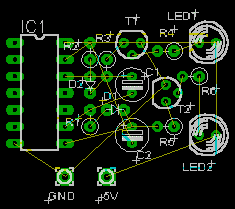
As the example, I use the pattern of "Let's try".

Route icon is used for the manual wiring.
After pushing Route icon, it sets a wiring attribute with the icon bar.

 Layer Layer |
This is the layer specification of the wiring to draw.
1 is the component side (auburn) and 16 is the wiring side (dark blue). |
| Bend Angle |
This is the bend angle specification of the wiring.
From left
 0 : Starting point - horizontal - vertical - end 0 : Starting point - horizontal - vertical - end
1 : Starting point - horizontal - 45° - end
2 : Starting point - end (straight connection)
3 : Starting point - 45° - horizontal - end
4 : Starting point - vertical - horizontal - end |
| Width |
This is the specification of the wiring width (thick).
The default unit is an inch. To change into the mm, it is by 25.4 times.
 |
| Inch | mm |
| 0.01 | 0.25 |
| 0.012 | 0.3 |
| 0.016 | 0.4 |
| |
| Inch | mm |
| 0.024 | 0.6 |
| 0.032 | 0.8 |
| 0.04 | 1.0 |
| |
| Inch | mm |
| 0.05 | 1.3 |
| 0.056 | 1.4 |
| 0.066 | 1.7 |
|
|
| Via shap |
Via is a through-hole for the connection between top wiring and bottom wiring.
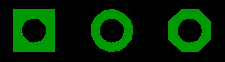
The shape of Via can be selected from three kinds. From left, Square, Round, Octagon.
 |
| Via diameter | This is the specification of the Via size. |
| Via drill diameter | This is the hole diameter specification of the Via. |
| Let's wire between the 7th pin of the IC and the ground terminal. I try the wiring which used Via for the practice. It wires on the wiring side from the 7th pin of the IC and on the way, it makes a component side wiring using Via. |
 Layer Layer | 16 Bottom |
| |
| Bend Angle | 1 |
| |
| Width | 0.04 |
|
 | 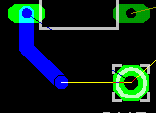 |
Click the 7th pin of the IC as the start point of the wiring. It is possible to draw wiring when moving a mouse pointer.
It isn't necessary to continue to push the button of the mouse. |
Click at the terminal or the relay point of the wiring. The wiring there is fix.
In case of relay, the fixed point becomes the following start point. |
Change a layer to Top from Bottom.
| Layer | 1 Top |
|
|
| Via shap | Octagon |
|
|
| Via diameter | Auto |
|
|
| Via drill diameter | 0.024 |
|
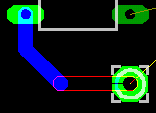 | 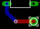 |
Move a mouse pointer to the ground terminal which is an end point.
The color of the wiring becomes the red which shows wiring at the component side. | Wiring is fixed when clicking a terminal. A Via which joins wiring between the wiring side and the component side is automatically added. |
 Ripup icon is used to return fixed wiring to the original un-wiring (thin yellow line) condition. Ripup icon is used to return fixed wiring to the original un-wiring (thin yellow line) condition.
As for Ripup, refer to "Rework of the pattern".
 Wiring is done according to the grid. The default grid interval is 0.05 inches. Wiring is done according to the grid. The default grid interval is 0.05 inches.
Because the pin interval of the DIP-type IC is 0.1 inches, so one wiring can be passed among the pins. I think that there is no problem in this setting generally. However, you can change it by View -> Grid... on the menu bar.
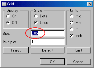 If you change the Size value, the grid interval can be changed.
|