Library making technique (6)
|
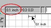
The part which is not in the library of EAGLE must be newly made by yourself. As for the new part data, the symbol data to use with the schematic and the pattern data to use with the board should be made first. After that, the device data that they were combined is made. The various techniques are necessary to make symbol data and package data. The techniques to introduce here are some of them. Please acquire the other techniques by yourself. Below, I will introduce about the making of a ultrasonic sonar as the example. I made the name of the library "15_sonar.lbr". As for the making of a library, look at "Creating of a new library".  Let's attempt to make symbol data first. It pushes the Symbol button and makes symbol data. This time, I made TX. The screen where grid line were drawn with 0.1 inches is indicated in the window.
 Wire function is used to draw a schematic symbol. Wire function is used to draw a schematic symbol.When pushing the Wire button, a tool bar like above is indicated at the top of the window. The symbol should be drawn in "94 Symbols" layer. EAGLE is managing various data with the layer. The data in each layer can do display or non-display independently. The symbol of the schematic is 94 layer. The button in the right is the button which selects the curve of the line. The thickness of the line can be designated by Width. I am using 0.005 inches for the lead wires and 0.01 inches for the symbol lines. When the pull-down menu doesn't have the value to want, the value can be directly set in the Width window. The point of the setting is to put a mouse pointer on the Width window during setting of a value. It isn't sometimes possible to set when removing a mouse pointer from the window. The line style can be selected in Style. Generally, Continuous is used.
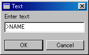
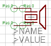
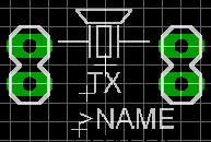
 It sets the designation of the name and the value of the part. Designation is described as the letter using the Text button. It sets the designation of the name and the value of the part. Designation is described as the letter using the Text button.The part name must be set to 95 and the value must be set to 96.
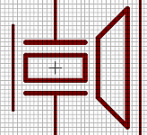
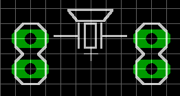
It sets Pin to connect with the other part to the created symbol data. This Pin is linked to Pad of the board at the device data. In case of this sonar part, two Pads are used for one wiring. So, two Pins of the symbol should be provided for one wiring. The Pin button is used for the pin to be additional. Following icon bar is indicated when pushing the Pin button. 
This time, I did the following setting to the terminal of the sonar.
Because Length is None, the setting of Orientation is the same anywhere. However, the position of the "Pas" changes with the setting of Orientation.
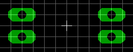
Four Pins are corresponding to four Pads on the board. The setting of Pin name is done by the Name button. It clicks Pin which sets or confirms a name by pushing the Name button. The setting window of Name is displayed by this. It sets a necessary name. 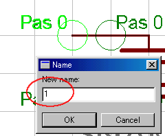 The making of symbol data ended above. I recommend data save at this point.  Let's make package data. It pushes the Package button and makes package data. I did to TX like the symbol. The screen where grid line were drawn with 0.05 inches is indicated in the window. In the pin interval of the DIP-type IC, it is 0.1 inches. So, it becomes the pin interval of the IC with 2 grids.
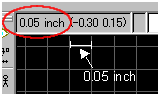
 To adjust a grid interval, select View -> Grid from the menu.  You can change a grid interval at the value of Size. When the set value is small, a grid line isn't indicated. Even if a grid line isn't displayed, the grid function is effective. It puts Pad which mounts a part first. When pushing the Pad button, a tool bar like above is indicated at the top of the window. The mark of five pieces of green on the left is the shape selecting button of Pad. It is a square, a round, an octagon, an X long octagon and a Y long octagon. The diameter of Pad can be set by Diameter. In case of the square, it is length with side. In case of the round, it is diameter. In case of octagon, it is length in the top and the bottom, on either side. In case of an X long octagon and a Y long octagon, it is length with short side. The setting unit is an inch. To change millimeter from inch, it does inches by 25.4 times. 0.05(inch) x 25.4 = 1.27(mm). In case of auto, the diameter of Pad is automatically set according to the setting size of Drill. Drill is the setting of the diameter of the hole. It should be set according to the diameter of the lead wire of the part. The setting unit is an inch. 0.032(inch) x 25.4 = 0.8(mm).
It is difficult to find the mounting place of the parts when there are a lot of pins on the printed board. Especially, when the package density of the part is high, the confusion is intense. It is possible for the confusion to decrease if the shape of the part is drawn. It becomes the reference of the putting of a part if the size of the part is drawn. It is also possible to prevent the defect of the mounting by the bump of the parts.  The Wire button is used to draw the shape of the part. The Wire button is used to draw the shape of the part.When pushing the Wire button, a tool bar like above is indicated at the top of the window. "21 tPlace" layer is used for the part shape. Where "t" is Top and is the component side of printed board. The wiring side is "22 bPlace". The function of the other button is the same as schematic symbol.
 In case of addition of the letters except name(>NAME) and value(>VALUE), it uses the Text button and adds them to the "21 tPlace" layer.
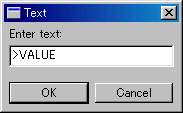
It sets the designation of the name and the value of the part. Designation is described as the letter using the Text button. The part name must be set to 25 and the value must be set to 27.
The setting of Pad name is done by the Name button. It clicks Pad which sets a name by pushing the Name button. The setting window of Name is displayed by this. It sets a necessary name.  The making of package data ended above. I recommend data save at this point. Device data is made with the combination of the symbol data and the package data. The device data is used for the parts adding to the schematic. By the device data, package data is automatically added to the board simultaneously with making of a schematic. As for the making of device data, refer to "Creating of device data". 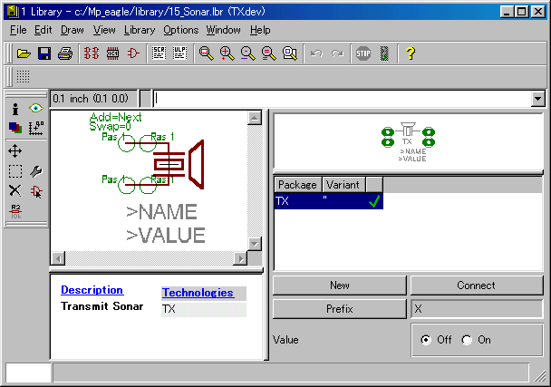 |