Library making technique (3)
|
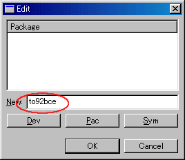
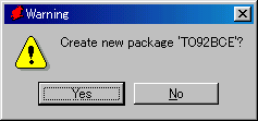
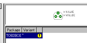
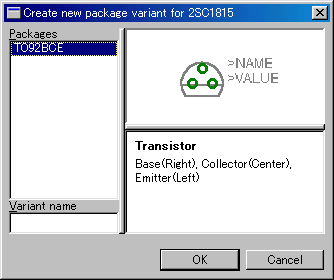
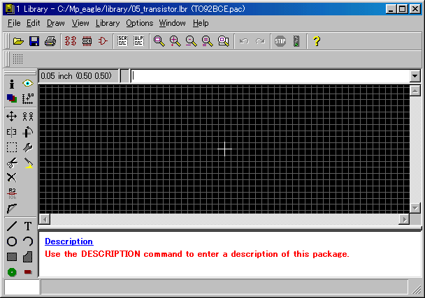
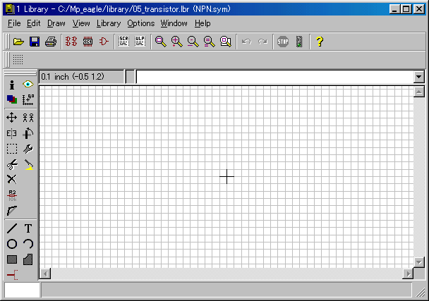
A command is used for the change of the part name in the library. There is Rename in Library of the menu bar but it doesn't operate normally. Bug ? I will explan using the capacitor library. There is named CAP-2,5 in the EAGLE default library. The pin interval of this capacitor is 2.5mm(0.1 inches). Because the pin interval of the IC is 0.1 inches, I will change this into the name which used INCH. I will change "CAP-2,5" into "CAP-0.1". Comma ( , ) is used for "2,5". 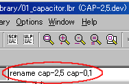 It inputs "rename The part name which is displayed in the title bar of the library editor window will be changed. The package name or the symbol name can be changed by same way. When the package name or the symbol name is changed, the linked name of the device data is changed automatically. Here, I will explain how to copy the parts which are in the other library onto own library. "The method for the library copy" is explaned on other page. Here, I will explan the method to creat new library.  It operates with File -> New -> Library with the control panel of EAGLE. The editorial window of the library is displayed by this operation. The path of the default library of EAGLE is displayed in the title of this window. It operates with File -> New -> Library with the control panel of EAGLE. The editorial window of the library is displayed by this operation. The path of the default library of EAGLE is displayed in the title of this window.However, you can save this library in your own library folder. I created new library of the name "05_transistor", under Mp_eagle\library with File -> Save as.... I will add the NPN type transistor named 2SC1815 to the new library. The structure type of this transistor is TO-92. First, it looks for the package data of TO-92. A file selection dialog is displayed by the Open icon or File -> Open. It selects "transistor-small-signal.lbr" from the default library of EAGLE. In my case, the file exists in "C:\Program Files\EAGLE-4.09r2\lbr\transistor-small-signal.lbr".  It clicks Package button and selects TO92A from displayed list.  It clicks Group icon and drags to surround all parts while pushing the left button of the mouse. 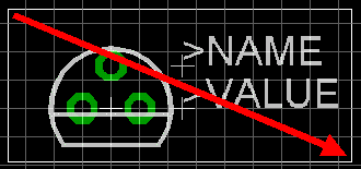 The parts which were selected by this operation become highlights (bright color).  Next, it clicks Cut icon and moves a mouse point onto the package window and it clicks the left button of the mouse. The package data which was selected by this operation is copied on to the clipboard of EAGLE.Don't forget clicking on the window. When doing this operation, because there is no change, it isn't possible to confirm that it was normally copied. The Cut button is used but the original package data doesn't disappear with this operation. Because the data on the clipboard of EAGLE disappears when it closes EAGLE, it must not close EAGLE until the data is pasted on new library. It isn't possible to use Copy icon for this operation. The Copy icon is the one to copy the object of the package. The whole part can not be copied. Next, it opens a copied library(New library). When selecting "Package" in the edit window of the copied library, the edit dialog of Package is displayed. It inputs a package name to the column of New and pushes the OK button. This time, I did to TO92BCE. BCE is to distinguish between the arrangement of the pad.
  When clicking Paste icon, the package data which was copied onto the screen is displayed. This data moves with the mouse point. It moves for the center of the data to become the position of the + mark at the center. Data is fixed when clicking the left button.
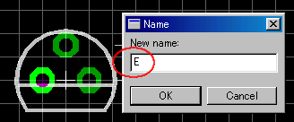
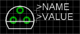 Package data was copied.  It confirms the pad name of the package data. Because this pad name is used for a link between the symbol and the pattern, it must set, being sure. Because the package data is a TOP VIEW of the part, don't make a mistake. The pad name of the package doesn't have to be the same as the pin name of the symbol. There is no problem if not making a mistake in the position of the pad. When seeing 2SC1815 from top, the left pad is an emitter, the topside is a collector and the right is a base. It confirms the pad name of the package data. Because this pad name is used for a link between the symbol and the pattern, it must set, being sure. Because the package data is a TOP VIEW of the part, don't make a mistake. The pad name of the package doesn't have to be the same as the pin name of the symbol. There is no problem if not making a mistake in the position of the pad. When seeing 2SC1815 from top, the left pad is an emitter, the topside is a collector and the right is a base.When clicking Name icon and clicking a pad (green), the name box of the pad is displayed.
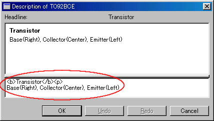
 It clicks Description in the window. It types a necessary description and pushes the OK button.
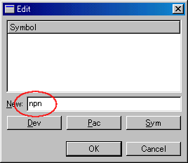
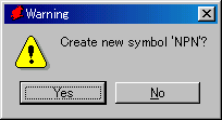
  It saves package data. Data is saved when clicking Save icon or selecting File -> Save. The copy of the symbol data is almost same as the operation of the package data. It opens the library of data to copy. This time, I selected "transistor-small-signal.lbr" from the default library of EAGLE.  It clicks Symbol icon and selects NPN from the displayed list.  It clicks Group icon and drags to surround all parts while pushing the left button of the mouse. 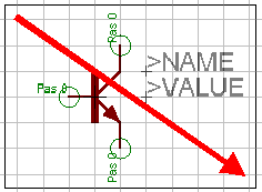 The parts which were selected by this operation become highlights (bright color).  Next, it clicks Cut icon and moves a mouse point onto the package window and it clicks the left button of the mouse. The package data which was selected by this operation is copied on to the clipboard of EAGLE. Next, it opens a copied library(New library). When selecting "Sumbol" in the edit window of the copied library, the edit dialog of Package is displayed. It inputs a symbol name to the column of New and pushes the OK button. This time, I did to NPN.
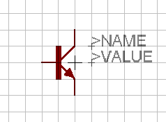
  When clicking Paste icon, the symbol data which was copied onto the screen is displayed. This data moves with the mouse point. It moves for the center of the data to become the position of the + mark at the center. Data is fixed when clicking the left button.
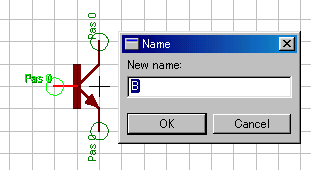
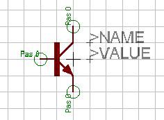 It confirms the pin name of the symbol data. When clicking Name icon and clicking a pin (green), the name box of the pin is displayed.
It saves symbol data. Data is saved when clicking Save icon or selecting File -> Save. The device data is the data which is made with the combination of the package data and the symbol data. This data can not be made with the copy of existing data. This time, I will create device data as 2SC1815.  When clicking Device icon with the library of 05_transistor, the edit dialog of Divice is displayed. It inputs a device name to the column of New and pushes the OK button. This time, I did to 2SC1815. 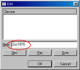 The confirmation message of the new data is displayed when pushing the OK button. 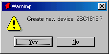 After confirming a name, it pushes the Yes button. 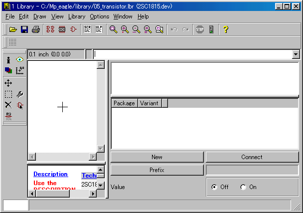
 First, it adds a symbol. When clicking the Add button, the selecting dialog of the symbol is displayed. This time, only NPN is registered. It selects NPN and pushes the OK button. When moving a mouse pointer to the symbol data display area, the symbol which moves with the mouse pointer appears. It moves a symbol to + at the center and fixes it with the left click of the mouse. When the symbol is small, the display can be expanded using the In icon. 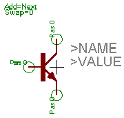 To stop a addition feature, it clicks the Cancel button.
It does the link of the pin of the symbol data and the pad of the package data.  The Connect button is used for the link of the data. When pushing the Connect button, following window is displayed. 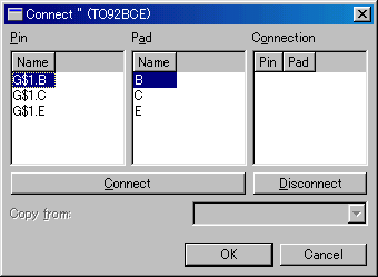
 The This means the link was done normally. 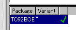 The prefix is the character to put to the head of the part name. Generally, R is used for the resistor and C is used for the capacitor. When more than one the same part is used, a number is put behind the prefix like R1, R2 and so on. The data which was created this time makes TR because it is a transistor. 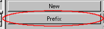 The Prefix button is used to put a prefix. 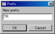 It is set when pushing to be OK. In EAGLE, a parts code like 2SC1815 is used as Value. When displaying a parts code in the schematic, it makes Value OFF. Seemingly, it feels as opposite. When Value is ON, Value isn't displayed in the schematic. In this case, Value can set by the Value button of the schematic. When making Value OFF, Value can't be changed in the schematic basically. In case of the resistor or the capacitor, it makes Value ON.
When trying to change Value (parts code) of the part which made Value OFF, following warning message is displayed. 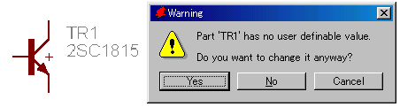 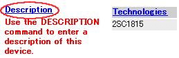 The description of the device can be set by Description. It clicks Description in the lower left window. This time, I set following description. 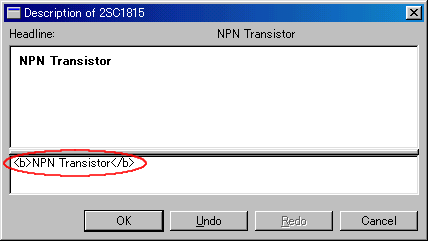 The display is as follows. 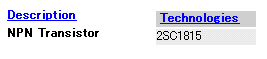 Headline of this description is displayed in the Description column when adding a part with the schematic. 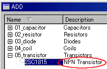 |