Circuit explanation for Count-down timer
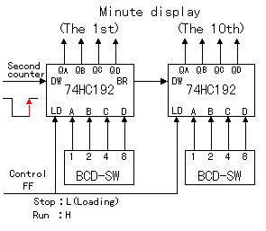 I am using 74HC192(Presettable Synchronous Up/Down BCD Counter) as the counter. There is 74HC190 and so on in the counter which can be downed in the count. I used this counter because I used the clear terminal as the second counter. The clear signal may be unnecessary. The pulse signal (being the once per minute) from the second counter is inputted to DW(Count Down). The counter is count-downed by the low to high transition of the signal. The output of BR(Borrow) becomes the L (the low level : 0 V) when the counter becomes 0. Next, it changes into H (the high level : +5 V) when the counter becomes 9. The counter of the upper palces is count-downed by the change of such BR. When the LD(Load) terminal is in the L condition, the original value of the counter can be set with BCD-SW. At the time of this condition, because the value which is the same as the set value of BCD-SW spreads through the display part, too, you can confirm the set value in the display part. Because the thumbwheel switch is used this time, you find the set value even if you don't confirm by the display. When the LD is not in the H condition, the counter doesn't work. The condition of the LD is controlled with the control circuit which is controlling the operation of the timer. The BCD(Binary Coded Decimal) counter is the counter which handles from 0 to 9. The counter of this kind has the binary counter as well as the BCD counter. The binary counter is the counter which handles from 0 to 15 and it says the hexadecimal (Hex) counter, too. 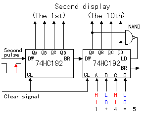 I am using 74HC192 as the second counter. The following of the 00 seconds is not the 99 seconds. The point in the second counter circuit is to make the 59 seconds next of the 00 seconds. The circuit is simple. The output of the NAND gate becomes in the L level when the 10th of the second display becomes 9. It inputs this output to LD(Load). The input of the presetting is set to the counter when the LD becomes the L level. The circuit this time sets "5" as the presetting. The output of the counter becomes "5" when "5" is set to the counter. With it, the output of the NAND gate becomes the H level. Because "5" was already set to the counter, there is not an influence. After that, the count-down is done from 5. The output of the counter becomes "9" momentarily but is immediately set to "5". You can not see the change. 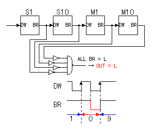 The L level is output by the BR terminal of the counter when the count value becomes 0. The BR signal of each counter is reversed by the inverter and is inputted to the NAND gate. Only when the BR terminal of all counters becomes the L level, the output of the NAND gate becomes the L level. 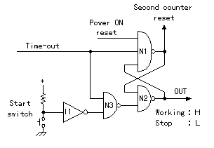 I am using the SR-type flip-flop(FF) which used the NAND gate as the circuit which controls the operation(start/stop) of the timer. I am using the SR-type flip-flop(FF) which used the NAND gate as the circuit which controls the operation(start/stop) of the timer.N1 is for the stop and N2 is for the start. As for the operation of the SR-type FF, see "The operation explanation of the D-type flip-flop". When the set value of the minute counter is not 00, the time-out signal becomes H. When the start switch is pushed at this time, the output of I1 becomes H and the output of N3 becomes the L. The output of N2 becomes H when the output of N3 becomes the L. The power ON reset signal becomes the L immediately after the turning on but after that, it becomes H. Because the time-out signal is H too, all input of N1 becomes H and the output of N1 becomes the L. The output of N1 is connected with the clear terminal of the second counter.The cleared condition is canceled when the clear terminal becomes the L. The output of N3 becomes H when the start switch becomes OFF. However, because the output of N1 is connected with the input of N2, the output of N2 is as the H condition. (Condition during the timer operation) The time-out signal becomes the L when the timer does the count-down and becomes the 00 minutes and the 00 seconds. With this, the output of N1 becomes H. Because the output of N3 is H, the output of N2 becomes the L. The output of N2 of the start/stop control circuit is connected with the LD(Load) terminal of the minute counters. The set value of the BCD switchs are set in the minute counters when this output becomes the L. Because it is, the time-out signal changes into H immediately from the L. The output(L) of N2 is connected with the input of N1. Even if the time-out signal changes to H, the N1 output is as the H condition. The second counter is reset when the output of N1 becomes H. When the start switch is OFF, the output of I1 is in the L condition. In this case, because the output of N3 is H, the output of N2 is as the L. (Timer stop condition) When the setting of the minute counter is the 00 minutes, the time-out signal is the L. When the start switch becomes ON in this condition, the output of I1 becomes H but because the time-out signal is the L, the output of N3 is H. The condition of N1 and N2 doesn't change. The timer is as the stop condition. The start switch circuit works at the subtle voltage. The small pull-up resistor value prevents the interference by the noise.(The extremely small value is worthless. Hundreds ohms equal to or more than.) When the wire to the switch is long, use the shielding wire. The start/stop control circuit does following control.
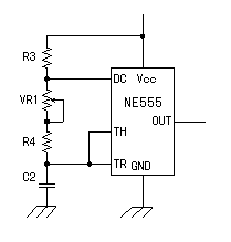 It is the oscillator which used NE555. It is the oscillator which used NE555.The roughly frequency can be calculated by the following formula. In the measurement, the frequency became approximately 1 Hz at VR1+R4 = 5.7k-ohm. Even if it considers the error of the parts, it is possible to adjust to the oscillation frequency of 1 Hz with the 1k-ohm variable resistor. The details of the oscillator by NE555 see "555 oscillator". 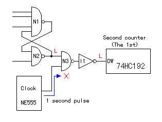 The pulse in the 1 second from the clock generator is inputted to the count-down terminal(DW) of the counter and the count-down is done. When becoming at 0'0", the count-down is made to stop. The stop of the count-down is done in making the input of N3 the L level. When making the counter stop, it makes the count-down terminal stop in the L level condition. When stopping in the H condition, the BR terminal of each counter runs out in the L condition. Therefore, the counter start can not be restrained in the setting in the 0 minutes. I wasn't considering this thing at the circuit which was made first. 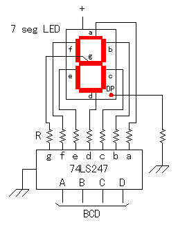 As the 7 segment LED, use the anode common type. The luminous brightness of the LED depends on the kind of the LED. When using the LED which is different kind like this time, change the value of the resistors to adjust the brightness. To adjust for the electric current in the one segment to become less than 10 mA is safe. Adjust the electric current in the same way with the resistor when making DP(Dot Point) light up, too. I used 74LS247 as the LED driver. As for the relation between the BCD input and the LED segment, see "Circuit explanation of Digital dial". 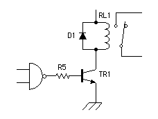 I used the relay to drive the outside circuit while the timer works. I used the relay to drive the outside circuit while the timer works.The drive electric current of the relay depends on the kind of the relay. The relay (G2VN-237P which is made from OMRON) which was used this time works in the about 30 mA electric current. The maximum output current at the NAND gate (74HC00) of the timer control circuit can not drive the relay directly because it is 4 mA. Therefore, it prepares the drive circuit which used the transistor (TR1). The DC Current Gain (hFE) of the transistor (2SC1815) which was used this time is about 100. It depends on the hFE Classification. The value of R5 is calculated as follows. The base electric current to pass the 30 mA electric current to the collector is 0.3 mA(300µA) because it is hFE=100. The voltage of the H level of the NAND gate is +5 V and VBE of the transistor (TR1) is about 0.6 V. Because it is, the voltage which is added to the R5 is 5V-0.6V = 4.4 V. The resistance value to pass the 0.3 mA electric current at this voltage becomes 4.4V/0.3mA = 14.7 k-ohm. To drive the relay at this value, there is not leeway. Therefore, I considered the output current at the NAND gate and made the R5 = 5.6 k-ohm. In case of this resistance value, the base electric current is 4.4V/5.6k-ohm = 0.79 mA. This electric current value is less than the permissible current value of the output of the NAND gate. In the calculation, the collector electric current flows by 79 mA. However, the electric current of 79 mA doesn't flow. It flows only to the drive electric current (about 30 mA) of the relay. That is, the transistor becomes the saturation state(Even if the base electric current changes little, the collector electric current doesn't change). In this condition, the voltage between the collector and the emitter is 0 V almost. When using the transistor circuit, it is necessary to consider that phase of the input and the output changes by the 180 degrees. When the output of the NAND gate is the H level, the collector voltage of the transistor becomes the L level (0V). 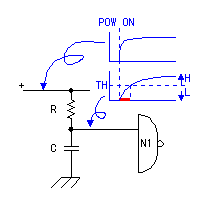 This is the circuit which initializes the timer when turning on. This is the circuit which initializes the timer when turning on.It is the simple circuit which used the capacitor and the resistor. The supply voltage rises when turning on. Immediately after the turning on, the electric charge isn't stagnant at the capacitor. Therefore, the voltage of the both edges of the capacitor doesn't rise immediately. The input of N1 becomes the L level below the threshold voltage. The flip-flop (FF) for the timer control is compulsorily set in the timer stop condition by it. When the electric charge finishes stagnating at the capacitor, the voltage of the capacitor rises and the reset operation ends. With it, the timer becomes the condition which can be the motion control. 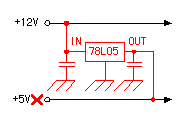 This time, the timer which I made is supplying +12 V and +5 V separately as the power supply. (It is because there was a power unit which both voltage can be supplied to.) This time, the timer which I made is supplying +12 V and +5 V separately as the power supply. (It is because there was a power unit which both voltage can be supplied to.)It uses the 3 terminal voltage regulator to work at only +12 V. When using the 3 terminal voltage regulator, don't supply the +5 V power supply from outside. When supplying +5 V from outside, don't mount the 3 terminal voltage regulator. |
||||||||||||||||||||||||||||||