Our first design attempt will be a Z80 running at 4 MHz, and having 64K of dynamic memory. We will provide an 8K EPROM for startup code. A CPU without I/O is worthless so we will also provide an SIO to connect a serial terminal to.
As promised, circuit 1 is fairly simple. Page 1 of the schematics shows the Z80 CPU. It uses a simple RC network to generate RESET*. If I were to start adding "whistles and bells", the first thing I would do is to generate RESET* with some kind of SCHMIDT TRIGGER gate. This would eliminate the slow rise time in the RESET* signal.
The clock to the Z80, and its' peripheral chips, is generated by an oscillator module. The traditional clock driver circuit is replaced by a modern CMOS inverter; a 74HCT14.
RESET* is generated by an RC network feeding a section of a 74HCT14, a Schmidt trigger inverter. The resulting signal is inverted again to retain the active low polarity of the reset signal.
Also on page 1 is the EPROM. It is an 8K device, a 2764/27C64. It will ONLY be used during startup. We will see how this is implemented when we examine the PAL equations a little later.
On page 2 we see the heart of the design, our DRAM controller. Since the Z80 can only address 64K of memory I decided that we would give it that much; in two parts. The 4464 is a 64K by 4 bit dram. Thus, two of these devices and we have a full 64KB of DRAM. That's not bad. It used to take a fairly large board to do that.
The DRAM timing is generated by the PAL, at U5. The PAL chosen for this design is a 16L8. This device was chosen because they are cheap and easy to work with. Next to the PAL you will notice a section of a D type flip-flop, U4. This is how we get the system started up.
When you power up the circuit, RESET* will go low for a time determined by the values of the components in the RC circuit on page 1. When RESET* goes low, the Q output of U4B will go high (on page 2). This signal is feed to the PAL. In the PAL equations, it is called STARTUP, and it is active high. The full PAL listing is attached, but let's examine the equations in detail.
/ROM = STARTUP * /MREQ * /RD ; ROM IS ONLY ENABLED DURING STARTUP
The equation shown above illustrates how STARTUP is used to allow access to the ROM. Note that ALL memory reads are directed to the ROM during startup. We didn't include any address lines in the equations. The idea here is to copy the contents of the ROM into the DRAM, then switch the ROM out. EPROMs draw a considerable amount of power. By switching it out, and not accessing it, the eprom will draw less power. Also, we simplify our memory control design. Since the Z80 can only address 64K of memory total, and we have 64K of DRAM plus 8K of ROM, we could have a sticky wicket indeed.
This eliminates that potential problem. Now we are fully flexible as to what we run in the DRAM. We would probably implement a monitor program to put in the ROM that would let us download other programs from a PC.
Continuing with our examination of the design for circuit 1, let's look at the DRAM controller. The entire DRAM circuit is presented on page 2 of the schematics. The address lines from the Z80 are multiplexed into the DRAM chips by the multiplexers at U7 and U9.
The outputs of the multiplexers drive the DRAM inputs through 22 ohm resitors. The inputs of dynamic memory devices present no significant current load to the driving circuitry, but they DO present a high capacitance load; usually on the order of 10pf per device pin. In the case of our simple design we have two parts. The address multiplexers each drive two pins, thus a total of 20pf of capacitive loading. A typical TTL output has a DC resistance to VCC or GROUND of something on the order of 50 ohms.
This resistance, coupled with the capacitance of the load, have two major effects on the waveforms driving your DRAM chips.
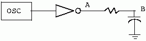
First, it tends to delay the waveform. As an experiment, feed a clock signal at 10MHZ into an RC network comprised of a 50 ohm resistor feeding a 100PF capacitor to ground, as in the following illustration.
After you wire the circuit in figure 23, connect a dual trace, 100MHZ, oscilloscope to points A and B. You will notice that the waveform at point B looks much like the waveform at point A, but is delayed in time. This is just one of the things that happens to your signals that are driving your memory devices.
The other thing that happens is that the signal at point B will not look EXACTLY like the signal at point A. It will have a slower rise and fall time. It takes time to charge and discharge the capacitance in the load. This time contributes to the delay effect you saw above, but it also decreases the rise and fall times of the signal. On your scope, the signal at point A will look almost vertical when it makes changes from high to low, and back again. The signal at point B will look more sloped. It takes longer to make the change from high to low and back again.
Every time the signal changes state, it has to deal with that nasty capacitance again. On a low to high transition, the capacitance has to be charged. On a high to low transition it has to be discharged.
Here, there is no substitute for brute force. In the schematic for circuit 1 you will notice that I drew a 74157, not a 74LS157. This was not an accident. The 74157 has more drive capability than its' 74LS157 equivalent. In making the "LS" line of TTL I.C.'s most manufacturers put resistors in series with the output transistors. This "softens" the output transitions. NOT what we want to drive DRAMs with. If you can't find the plain 74157's, try the 74F157's. They have the resistors, but are speeded up so that they will generally work well.
In addition to having to deal with the delaying effect of the capacitance, and the slowing effect it has on our waveforms, there is also ringing to worry about. At the speeds these signals transition (in excess of 100MHZ) we get a transmission line effect.
In addition to the RC we have that is formed by the resistance in the driver output, and the capacitance of the load, now we have a coil introduced by the etch that connects the driver to the memory array, or worse, the wire-wrap wire.
As we all now from our basic electronics you can store energy in a coil. When we charge the capacitance of our load, current flows in the coil. When the coil discharges a voltage is generated in it that is the opposite polarity of that which charged it. The current generated is also out of phase with the transition. Now we have a classic RF circuit.
The worst case for us is the high to low transition. The ringing generated by all of this can drive the signal well below ground. Very few I.C.'s will really like this. In fact, it can destroy some devices; especially older DRAM chips. When an input is taken below ground, the chip can become reverse biased, and "turn on" like an SCR. Like an SCR, when this happens, the only way to turn it back of is to remove power. For some devices there is no way you can remove power fast enough to prevent permanent damage, even if you knew that it had gone into SCR mode, which you probably won't. Usually the first indication you get is that awful smell of burning I.C.'s. If you don't know what that smells like, good.
We will deal with ways to minimize this effect later, but, for now, let's just try to dampen it. That is the purpose of the 22 ohm resistors in series with the 74157 outputs. They are not in series between VCC and the output transistor, so they don't effect our rise or fall times. Their purpose is to dampen the ringing on these lines.
For a memory array this small, they could have probably been left out. I included them here to teach proper design practices. Our goal here is not to save a few pennies on resistors, it is to design something that actually has a chance to work.
To continue with the analysis of our design let's look at how the DRAM timing is generated. Consider the following equations with me.
/RAMSEL = /MREQ * RFSH           ; THE WHOLE 64K IS DRAM
        + /MREQ * /RFSH          ; REFRESH
To control DRAMs we need to generate RAS*, and CAS*. We also have to generate a signal to control the multiplexers, the 74157's. The DRAM timing begins with MREQ* from the Z80. This indicates a memory access. The signal RAMSEL is generated from MREQ*. At first glance it would seem that there is a redundant term in the equation for RAMSEL above. Did you catch it? RAMSEL is generated when RFSH is high, and when it is low. This would tend to say you could eliminate the RFSH term from the equation, but you really can't. They don't both have the same timing.
RAMSEL drives a delay line external to the PAL. Delay lines are very convenient to work with. This one would have 25ns between taps. This delay would satisfy most modern DRAM devices with access times of 150ns or afster. If you were trying to use slower devices then that you might have to chose different taps.
The first tap of the delay line is used to control the multiplexers. This signal is sometimes called MUX.
The second tap is fed back into the PAL and used to generate DRAM timing. At this point, we haven't really generated any DRAM timing, but all the players are in place. In the following equations we will actually generate RAS and CAS.
/RAS = /MREQ * STARTUP * /WR * RFSH ; ONLY DO WRITES DURING STARTUP
     + /MREQ * /STARTUP  * RFSH     ; ALL ACCESSES AFTER STARTUP
     + /MREQ * /RFSH * /CASIN       ; REFRESH

/CAS = RFSH * /CASIN * /RD * /STARTUP ; NORMAL CAS FOR MEMORY READ
AFTER
                                      ; STARTUP
     + RFSH * /CASIN * /WR       ; HOLD OFF CAS FOR EARLY WRITES
     + /RFSH * /MREQ             ; CAS GOES LOW EARLY FOR REFRESH
Whew! We finally did it. We got around to generating the memory timing. Did you catch it? Ok. We'll slow down and do it again. For a normal memory access we want to generate a RAS signal, followed by MUX, and finally CAS. We have a couple of special cases to think about though. We have refresh to do, and our special case for startup. During startup we can write to DRAM memory, but we can't read it. Reads go to the ROM. How can this possibly be useful? Hopefully it will all make sense soon. Hang in there with me.
For a normal access we need to generate RAS first. This is generated from MREQ. If STARTUP is high we will only generate a RAS during a write. We can see this in the first term of the RAS equation. After we get started up STARTUP will go low. From then on we use the second term. As long as RFSH is high we have a normal memory access. In this case RAS is basically generated from MREQ. We'll cover refresh in a little bit.
To generate CAS we use the CAS equation. If STARTUP is high reads are blocked. Note in the first term of the CAS equation that STARTUP must be low during a read cycle. For a write CAS is held off until WR goes active. We are using DRAM devices with common I/O pins, so we MUST implement early write. Holding off CAS until WR goes active does this for us. WR from the Z80 goes directly to the memory array. When CAS is generated there will be a delay of one PAL propagation time between when WR goes low, and when CAS will go low. This satisfies the setup time requirement on the DRAMs WE pin.
To complete the startup of our design we need a small piece of code. Consider the following.
;
; STARTUP CODE FOR CIRCUIT 1
;
ORG   0
; THE Z80 GOES HERE ON RESET
;
START:   LD   DE, 0     ; DESTINATION ADDRESS
         LD   HL, 0     ; SOURCE ADDRESS
         LD   BC, 2000H ; LENGTH
         LDIR           ; COPY IT
         OUT (0FFH), A  ; KICK OUT THE ROM
The above code listing is a very simple way to get our little Z80 started up. At RESET* the flip-flop at U4B was set presenting the signal STARTUP to the PAL. In this mode we can read from the ROM and write to the DRAM. The startup code simply copies code starting at zero in memory, to zero in memory, for the length of the rom. Thus. every rom location will be read, then written to the same address in the DRAM. Finally, an output instruction was executed to switch the rom out. Note that IORQ* is tied to the clear pin of U4B. When the output instruction is executed it pulses the flip-flop.
The next instruction will be fetched from the DRAM. STARTUP will be low, and that will satisfy the RAS equation in the PAL. From now until the next RESET* the Z80 will run from DRAM.
Now all we have to do is keep the DRAM refreshed. The Z80 was designed to refresh dynamic memories. Unfortunately that was almost 20 years ago, and the popular DRAM then was 16K by 1. The Z80 doesn't provide enough address bits to refresh modern DRAMS using RAS only refresh. So, what do we do. Well, all is not lost. We can use the refresh signal from the Z80 to trigger our refresh, but not to use the Z80's refresh address. That will work.
As we learned earlier, there are two ways to refresh dynamic memory; RAS only, and CAS before RAS. The Z80 was designed to work with RAS only refresh. This is not too surprising as that was all we had back then. The DRAM chip I chose for this design will support CAS before RAS refresh. Whenever possible we should use this because it reduces the parts count and complexity of our design.
The CAS before RAS refresh is all handled inside our PAL. Let's look at those equations again.
/RAS = . . . .
       . . . .
   + /MREQ * /RFSH * /CASIN     ; REFRESH

/CAS = . . . .
       . . . .
   + /RFSH * /MREQ              ; CAS GOES LOW EARLY FOR REFRESH
Above we see only the refresh portions of the RAS and CAS equations. When the Z80 wants to do a refresh it will signal this by asserting (taking low) both MREQ* and RFSH*. When we see this look what happens. CAS is generated from MREQ* instead of RAS. RAS is generated from CASIN, which comes from the second tap on the delay line. That's all there is to it. Done. CAS will go low first, then RAS. The multiplexers will switch when MUX changes, but we don't care. When CAS goes low first the DRAM ignores what is on its address pins. Refresh is fully taken care of.
We have spent quite a lot of time on page 2 of the design because that is where the DRAM timing gets handled, and this paper IS about doing just that; interfacing DRAMS to the Z80. On page 3 we see the implementation of our SIO. It turns out that using the SIO means that we need a CTC as well. After all, we need something to generate baud rate clocks for the SIO don't we?
Simple chip select signals are generated for these devices in the PAL. The Z80 address lines are not fully decoded to save pins on the PAL. The equations for these chip selects are as follows.
/SIO = /IORQ * M1 * /A07 * /A06  ; SIO AT 00H

/CTC = /IORQ * M1 * /A07 * A06   ; CTC AT 40H
Pretty simple huh? Can you tell me why I included M1* in these equations? You would see some very strange things happening if you didn't; just about the time you started to use the interrupt capabilities of the SIO or the CTC. The Z80 signals an interrupt acknowledge by executing a bus cycle with both M1* and IORQ* low. This is normally a mutually exclusive condition. M1 signals an instruction fetch cycle while IORQ signals an I/O cycle. When they go low together it is an interrupt acknowledge cycle.
The Z80 peripheral chips decode this internally and place their interrupt vector on the bus. Blocking the chip select prevents a spurious write to one of the chips registers, or to another I/O device you may wire into the circuit.
Z80 interrupts are wired in our sample circuit. The INT pin of both the CTC and the SIO are connected to the INT pin of the Z80. There is a 10K pullup on this line. The INT pins of all the Z80 family parts are open drain. That means they can pull the line low, but they can't force it high. This allows a daisy chain structure to work.
The interrupts are prioritized by the way the enable pins of the peripheral chips are wired. Note that the SIO has its' IEI, or Interrupt Enable In pin, tied high. That makes it the highest priority device in the interrupt chain. The IEO, or Interrupt Enable Out, pin from the SIO is connected to the IEI pin of the CTC. If there were another device, a PIO for example, the IEO from the CTC would go to the IEI of the PIO.
There is a limit to how far this can be carried. You can only connect four devices in this manner. It takes time for the enables to trickle down the chain and it has to be complete early in the interrupt acknowledge cycle. Then the correct will be able to place its' vector on the bus at the right time.
This concludes our analysis of circuit 1. We have implemented a simple Z80 with 64K of DRAM. To make the circuit more useful you would probably want to add some more I/O to it.
/* Also: CKT1.PDS and compiled JEDEC: CKT1.JED */
;PALASM Design Description
;---------------------------------- Declaration Segment ------------
TITLE    SAMPLE Z80 DESIGN # 1 SYSTEM TIMING CONTROLLER
PATTERN  Z80-1
REVISION A
AUTHOR   TIM OLMSTEAD
COMPANY
DATE     09/20/96
CHIP     PAL1  PAL16L8
;---------------------------------- PIN Declarations ---------------
PIN  1          MREQ                            ; INPUT
PIN  2          CASIN                           ; INPUT
PIN  3          A07                             ; INPUT
PIN  4          A06                             ; INPUT
PIN  5          RD                              ; INPUT
PIN  6          IORQ                            ; INPUT
PIN  7          M1                              ; INPUT
PIN  8          RFSH                            ; INPUT
PIN  9          WR                              ; INPUT
PIN  10         GND                             ; INPUT
PIN  11         PIN11                           ; INPUT
PIN  12         CAS                  COMBINATORIAL ; OUTPUT
PIN  13         RAS                  COMBINATORIAL ; OUTPUT
PIN  14         STARTUP                         ; INPUT
PIN  15         PIN15                           ; INPUT
PIN  16         CTC                  COMBINATORIAL ; OUTPUT
PIN  17         SIO                  COMBINATORIAL ; OUTPUT
PIN  18         ROM                  COMBINATORIAL ; OUTPUT
PIN  19         RAMSEL               COMBINATORIAL ; OUTPUT
PIN  20         VCC                             ; INPUT
;----------------------------------- Boolean Equation Segment ------
EQUATIONS
/RAMSEL = /MREQ * RFSH           ; THE WHOLE 64K IS DRAM
        + /MREQ * /RFSH          ; REFRESH

/ROM = STARTUP * /MREQ * /RD     ; ROM IS ONLY ENABLED DURING STARTUP

/RAS = /MREQ * STARTUP * /WR * RFSH ; ONLY DO WRITES DURING STARTUP
     + /MREQ * /STARTUP          ; ALL ACCESSES AFTER STARTUP
     + /MREQ * /RFSH * /CASIN    ; REFRESH

/CAS = RFSH * /CASIN * /RD * /STARTUP ; NORMAL CAS FOR MEMORY READ AFTER
                                      ; STARTUP
     + RFSH * /CASIN * /WR       ; HOLD OFF CAS FOR EARLY WRITES
     + /RFSH * /MREQ             ; CAS GOES LOW EARLY FOR REFRESH

/SIO = /IORQ * M1 * /A07 * /A06  ; SIO AT 00H

/CTC = /IORQ * M1 * /A07 * A06   ; CTC AT 40H