This application note presents programming techniques for reading an external voltage by employing bitstream continuous calibration in order to create a simple, inexpensive 8-bit 1 analog to digital converter with an input range of 0-5V. This implementation uses the SX's internal interrupt feature to allow background operation of the code as a virtual peripheral, and uses the Parallax demo board, taking advantage of Parallax' SX demo software user interface and UART features to allow the SX to communicate simply and directly with a personal computer via a serial RS232C port.
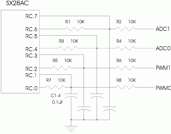
Figure 1 - Parallax demo board ADC/PWM circuit diagram
;******************************************************************************
;       Virtual Peripheral: Analog to Digital Converters
;
;
;       Length: 36 bytes (total)
;       Authors: Chip Gracey, President, Parallax Inc.
;		   modified by Craig Webb, Consultant to Scenix Semiconductor, Inc.
;       Written: 97/03/10 to 98/6/03
;
;******************************************************************************
;
;****** Assembler directives
;
; uses: SX28AC, 2 pages of program memory, 8 banks of RAM, high speed osc.
;       operating in turbo mode, with 8-level stack & extended option reg.
;
		DEVICE  pins28,pages2,banks8,oschs
		DEVICE  turbo,stackx,optionx
		ID      'ADCS'			;program ID label
		RESET   reset_entry             ;set reset/boot address
;
;******************************* Program Variables ***************************
;
; Port Assignment: Bit variables
;
adc0_out_pin    EQU     rc.4                    ;ADC0 input pin
adc0_in_pin     EQU     rc.5                    ;ADC0 output/calibrate pin
adc1_out_pin    EQU     rc.6                    ;ADC1 input pin
adc1_in_pin     EQU     rc.7                    ;ADC1 output/calibrate pin
;
;
;****** Register definitions (bank 0)
;
		org     8                       ;start of program registers
main            =       $                       ;main bank
;
temp            ds      1                       ;temporary storage
byte            ds      1                       ;temporary UART/I2C shift reg.
flags           DS      1                       ;program flags register
;
delay1		DS	1			;temporary delay variable
delay2		DS	1			;temporary delay variable
;
		org     50h                     ;bank2 variables
analog          =       $                       ;pwm and ADC bank
;
port_buff       ds      1                       ;buffer - used by all
adc0            ds      1                       ;adc0 - value
adc0_count      ds      1                       ;     - real-time count
adc0_acc        ds      1                       ;     - accumulator
adc1            ds      1                       ;adc1 - value
;adc1_count     ds      1                       ;     - real-time count
adc1_acc        ds      1                       ;     - accumulator
;
;
int_period	=       163                     ;period between interrupts
;
;**************************** INTERRUPT CODE *******************************
;
; Note: The interrupt code must always originate at 0h.
;       Care should be taken to see that any very timing sensitive routines
;       (such as adcs, etc.) are placed before other peripherals or code
;       which may have varying execution rates (like the UART, for example).
;
interrupt       ORG     0                       ;interrupt starts at 0h
;
;
;***** Virtual Peripheral: Bitstream Analog to Digital Converters
;
; These routines allow an 8-bit value to be calculated which corresponds
; directly (within noise variation limits) with the voltage (0-5V) present
; at the respective adc port input pins. These routines are timing critical
; and must be placed before any variable-execution-rate code (like the UART,
; for example). The currently enabled routine (version A) has been optimized
; for size and speed, and RAM register usage, however a fixed execution rate,
; yet slightly larger/slower routine (version B) is provided in commented
; (disabled) form to simplify building other timing-critical virtual
; peripheral combinations (i.e. that require fixed rate preceeding code).
;    Note: if version B is selected, version A must be disabled (commented)
;
;       Input variable(s) : adc0,adc0_acc,adc0_count,adc1,adc1_acc,adc1_count
;       Output variable(s) : pwm port pins
;       Variable(s) affected : port_buff, pwm0_acc, pwm1_acc
;       Flag(s) affected : none
;	Size (version A) : 9 bytes + 7 bytes (per pwm)
;			   + 2 bytes shared with adc code (see below)
;	Size (version B) : 6 bytes + 10 bytes (per pwm)
;			   + 2 bytes shared with pwm code (see below)
;       Timing (turbo)
;		version A : 2 cycles shared with pwm code (see below) +
;			   (a) [>99% of time] 11 cycles + 4 cycles (per adc)
;			   (b) [<1% of time] 9 cycles + 7 cycles (per adc)
;		version B : 6 cycles + 10 cycles (per adc)
;			    + 2 cycles shared with pwm code (see below)
;
:set_analog	bank    analog                  ;switch to adc/pwm bank
		clr     port_buff               ;clear pwm/adc port buffer
:adcs           mov     w,>>rc                  ;get current status of adc's
		not     w                       ;complement inputs to outputs
		and     w,#%01010000            ;keep only adc0 & adc1
		or      port_buff,w             ;store new value into buffer
:update_RC	mov     rc,port_buff            ;update cap. discharge pins

;
; VERSION A - smaller, quicker but with variable execution rate
;
:adc0           sb      port_buff.4             ;check if adc0 triggered?
		INCSZ   adc0_acc                ;if so, increment accumulator
		INC     adc0_acc                ; and prevent overflowing
		DEC     adc0_acc                ; by skipping second 'INC'

:adc1           sb      port_buff.6             ;check if adc1 triggered
		INCSZ   adc1_acc                ;if so, increment accumulator
		INC     adc1_acc                ; and prevent overflowing
		DEC     adc1_acc                ; by skipping second 'INC'

		INC     adc0_count              ;adjust adc0 timing count
		JNZ     :done_adcs              ;if not done, jump ahead
:update_adc0	MOV     adc0,adc0_acc           ;samples ready, update adc0
:update_adc1	MOV     adc1,adc1_acc           ; update adc1
:clear_adc0	CLR     adc0_acc                ; reset adc0 accumulator
:clear_adc1	CLR     adc1_acc                ; reset adc1 accumulator
;
; <end of version A>
;
; VERSION B - fixed execution rate
;
;*** The "adc1_count" register definition in the analog bank definition
;*** section must be enabled (uncommented) for this routine to work properly
;
;:adc0		sb	port_buff.4		;check if adc0 triggered
;		INCSZ   adc0_acc                ;if so, increment accumulator
;		INC     adc0_acc                ; and prevent overflowing
;		DEC     adc0_acc                ; by skipping second 'INC'
;		mov	w,adc0_acc		;load W from accumulator
;		inc	adc0_count		;adjust adc0 timing count
;		snz				;are we done taking reading?
;		mov	adc0,w			;if so, update adc0
;		snz				;
;		clr	adc0_acc		;if so, reset accumulator
;
;:adc1		sb	port_buff.6		;check if adc1 triggered
;		INCSZ   adc1_acc                ;if so, increment accumulator
;		INC     adc1_acc                ; and prevent overflowing
;		DEC     adc1_acc                ; by skipping second 'INC'
;		mov	w,adc1_acc		;load W from accumulator
;		inc	adc1_count		;adjust adc1 timing count
;		snz				;are we done taking reading?
;		mov	adc1,w			;if so, update adc1
;		snz				;
;		clr	adc1_acc		;if so, reset accumulator
;
; <end of version B>
;

:done_adcs

		mov     w,#-int_period          ;interrupt every 'int_period' clocks
:end_int	retiw                           ;exit interrupt
;
;******	End of interrupt sequence
;
;***************************** SUBROUTINES *********************************
;
;***************************** MAIN PROGRAM CODE ******************************
;
;		ORG     100h
;
; Program execution begins here on power-up or after a reset
;
reset_entry
		clr     rc                      ;initialize port RC
		mov     !rc,#%10101010          ;Set RC in/out directions
		mov     m,#$D                   ;set input levels
		mov     !rc,#0                  ; to cmos on port C
		mov     m,#$F                   ;reset mode register
		CLR     FSR                     ;reset all ram starting at 08h
:zero_ram       SB      FSR.4                   ;are we on low half of bank?
		SETB    FSR.3                   ;If so, don't touch regs 0-7
		CLR     IND                     ;clear using indirect addressing
		IJNZ    FSR,:zero_ram           ;repeat until done

		mov     !option,#%10011111      ;enable rtcc interrupt
;
; Main Program Loop
;
:loop		MOV	W,adc0			;get adc0 value
;
; <program code goes here>
;
		JMP     :loop                   ;back to main loop
;
;***************
		END                             ;End of program code
The circuit is a simple resistor capacitor network on each adc port pin (see figure 1). Essentially, the program code calculates the charge vs. discharge rates of the capacitor, according to the voltage (0-5V) applied to the corresponding adc input. Port pins RC.5 and RC.7 are both inputs which trigger when the capacitor is half charged. This is because, using mode register function 0Dh in the initialization section of the main program code, port pin input and outputs on port RC are set CMOS levels.
The interrupt code segment uses the bitstream continuous calibration approach to calculate the capacitor charge/discharge timing. The method is a rather unique one, which uses one port to monitor the capacitor level, and another as an output to charge and discharge the capacitor to keep it hovering at the input trigger level. The charging and discharging times depend on the voltage being applied to the corresponding adc input, and hence by measuring the charge time vs. (charge + discharge) time ratio, we can determine the voltage present at the adc input. The resolution of such a method is proportional to the calibration frequency, and due to circuit noise, the last few bits ( + 1 or 2 LSB's) must usually be thrown away.
Using adco as our example, the adc routine keeps count in the adc0_acc register of the number of times the adc input (port pin RC.5) is triggered high during 256 passes through the interrupt (the count of the number of passes being kept in the adc0_count register). The ratio of these two values gives the proportion of Vcc present at the adc0 input.
adc0_acc / adc0_count = Vadc0_nput / Vdd
| * Note: the original SX demo code erroneously returns an adc value of 0 for input voltages ³ Vdd |
In this implementation, a sample is taken as soon as adc0_count rolls over from 255 to 0, whereupon the value contained in adc0_acc is copied to adc0. This value, ranging from 0-255 *, directly corresponds to an input voltage of 0-5 volts, with a value of 0 representing 0 volts and a value of 0FFh representing 5V. It should be noted that with no input voltage present the input floats around (or very near to) a value of 7Fh, though slight offsets may result due to variations between what should be equal values for the resistors R3 and R4.
The resistor capacitor combination shown allows sampling of the incoming signal by the bitstream continuous calibration method described above, yet it also draws current from the input source in order to maintain the calibration at 0.5V dd . The effect of this is equivalent to having the input source connected through R4 (in this case a 10kW resistor) to 2.5 volts, so current drain considerations on the input source should be kept in mind.
| 2 Due to Nyquist's theorem, useful information can only be obtained for frequencies £ half of the sampling (or, in this case, the calibration) frequency. |
For adc0, SX port pin RC.6 is essentially acting like a auto-calibrating pulse width modulation output which keeps the capacitor at 0.5V cc using real-time feedback from port pin RC.7. This method for analog to digital conversion is effective for inputs whose highest frequency component is lower than half2 of the lowest frequency component of the calibrating pwm signal.
| 3 With an input voltage just under 5 volts, the pwm calibration output will only toggle high for 1 out of every 256 interrupt passes. With the input at (or over) 5 volts, the calibration output will remain low. For an input voltage slightly over 0 volts, the pwm calibration output will toggle low only 1 of every 256 passes, and with the input at (or below) 0V, the calibration output will remain high. |
The length of the pwm cycle varies, depending upon the voltage of the input, but the worst case is a pwm that toggles only once every 256 interrupt passes 3.
We can calculate the period between interrupt passes as follows:
| The interrupt is triggered each time the RTCC rolls over (counts past 255 and restarts at 0). By loading the OPTION register with the appropriate value, the RTCC count rate is set to some division of the oscillator frequency (in this case they are equal), which is the external 50 MHz crystal in this case. At the close of the interrupt sequence, a predefined value is loaded into the W register using the RETIW instruction, which determines the period of the interrupt in RTCC cycles. |
period (sec) = mode * prescaler * RETIW value / osc. frequency, where mode=1 (turbo) or =4 (normal)
So, for the worst case of 256 interrupt passes, at a crystal frequency of 50 MHz, in turbo mode, with a prescaler of 1, and with an RETIW value of 163, the lowest frequency present in the pwm signal is:
frequencypwm_min = 1 / period * 256 = 50 MHz / (1 * 1 * 163 * 256 ) = 1.2 kHz
| 4 In practice, even signals at or near this frequency will not sample with 8 bits of resolution. |
By this we can see that the adc will be able to monitor signals at or below4 fadc_max = 1.2kHz / 2 = 600 Hz.
| 5 For signals that vary within a minimal range about the 1/2Vdd calibration point, higher frequencies may be successfully monitored. |
At frequencies above5 this, not only will the adc begin to provide inaccurate information, but there will also be an increasing current drain on the incoming signal as the impedance to ground of the RC combination decreases.
Since timing is critical for accurate readings, all efforts should be made to make sure that any code executed in the interrupt prior to the adc code section maintains a uniform execution rate at all times. This can be done by placing it before any varying-execution-rate, state-dependent code (it should always come before the UART, for instance).
The Parallax demo board is designed so that port pins pwm0 and pwm1 can be swapped for adc's simply by adjusting the program code to remove the pwm interrupt section, adding code to the :adcs section such that adc2 and adc3 use port RC pins for pwm0 and pwm1, respectively, and by adjusting the register definitions appropriately. An example of the code follows:
analog		=	$	;adc bank
;
port_buff	ds 	1 	;buffer - used by all
adc0 		ds 	1 	;adc0 - value
adc0_acc 	ds 	1 	; - accumulator
adc1 		ds 	1 	;adc1 - value
adc1_acc 	ds 	1 	; - accumulator
adc2 		ds 	1 	;adc2 - value
adc2_acc 	ds 	1 	; - accumulator
adc3 		ds 	1 	;adc3 - value
adc3_acc 	ds 	1 	; - accumulator
adc_count 	ds 	1 	;adc calibration count
...
;
; <all pwm code removed>
;
:adcs 	MOV 	W,>>RC 		;get current status of adc's
	NOT 	W		;complement inputs to outputs
	AND 	W,#%01010000 	;keep only adc0 & adc1
	OR 	port_buff,W 	;store new value into buffer
	MOV 	RC,port_buff 	;update cap. discharge pins

:adc0 	SB 	port_buff.4 	;check if adc0 triggered?
	INCSZ 	adc0_acc 	;if so, increment accumulator
	INC 	adc0_acc 	; and prevent overflowing
	DEC 	adc0_acc 	; by skipping second 'INC'

:adc1 	SB 	port_buff.6 	;check if adc1 triggered
	INCSZ 	adc1_acc 	;if so, increment accumulator
	INC 	adc1_acc 	; and prevent overflowing
	DEC 	adc1_acc 	; by skipping second 'INC'

:adc2 	SB 	port_buff.0 	;check if adc2 triggered
	INCSZ 	adc1_acc 	;if so, increment accumulator
	INC 	adc1_acc 	; and prevent overflowing
	DEC 	adc1_acc 	; by skipping second 'INC'

:adc3 	SB 	port_buff.2 	;check if adc3 triggered
	INCSZ 	adc1_acc 	;if so, increment accumulator
	INC 	adc1_acc 	; and prevent overflowing
	DEC 	adc1_acc 	; by skipping second 'INC'

	INC 	adc_count 	;adjust adc's timing count
	JNZ 	:done_adcs 	;if not, jump ahead
	MOV 	adc0,adc0_acc 	;update adc0
	MOV 	adc1,adc1_acc 	;update adc1
	MOV 	adc2,adc2_acc 	;update adc2
	MOV 	adc3,adc3_acc 	;update adc3
	CLR 	adc0_acc 	;reset adc0 accumulator
	CLR 	adc1_acc 	;reset adc1 accumulator
	CLR 	adc2_acc 	;reset adc2 accumulator
	CLR 	adc3_acc 	;reset adc3 accumulator
:done_adcs
...
| file: /Techref/scenix/lib/io/adc_vp.htm, 18KB, , updated: 2002/3/12 21:34, local time: 2025/10/8 23:36,
216.73.216.137,10-3-124-149:LOG IN
|
| ©2025 These pages are served without commercial sponsorship. (No popup ads, etc...).Bandwidth abuse increases hosting cost forcing sponsorship or shutdown. This server aggressively defends against automated copying for any reason including offline viewing, duplication, etc... Please respect this requirement and DO NOT RIP THIS SITE. Questions? <A HREF="http://techref.massmind.org/techref/scenix/lib/io/adc_vp.htm"> Ubciom ADC Input VP - A Virtual Peripheral ADC: Using Bitstream A-to-D Conversion</A> |
| Did you find what you needed? |
Welcome to massmind.org! |
Welcome to techref.massmind.org! |
.