Circuit explanation
for the infrared sensor unit
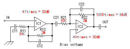 It uses 2 stages of the operational amplifiers and it about 1600 times amplifies the signal which was detected with the infrared sensor. Each stage does about 40 times of amplification. When saying correctly, the 1st stage is (1+R12/R11)=41 times because it is the noninverting gain amplification and the 2nd stage is (R22/R21)=40 times because it is the inverting gain amplification. To make detect only the move of the person or the animal as much as possible, it is making the amplifier have the band pass filter (BPF) function which used the resistor and the capacitor. As for the operation of the band pass filter by the operational amplifier, refer to "The band pass filter which used the operational amplifier". The band pass filter is the filter to make pass the frequency which is put between the low cut-off frequency (foL) and the high cut-off frequency (foH). 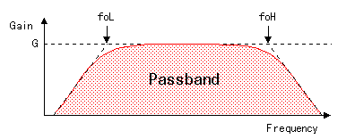 Each cut-off frequency can be calculated by the following formula. Each cut-off frequency can be calculated by the following formula.It is as follows when using the value of the 1st stage. 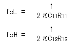 It is as follows when calculating the 1st stage.
The amplification circuit this time amplifies the signal of the frequency among from about 0.3 Hz to 8 Hz. It is not that the frequency except this band isn't amplified. It is the frequency which begins to become that it is difficult to be amplified.The condition : C11 = 10µF, R11 = 51K-ohm, C12 = 0.01µF, R12 = 2M-ohm 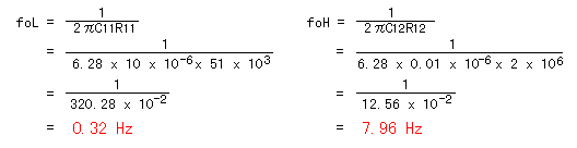 It is preventing detecting the change which was slowly or the too quick change by this band pass filter. To detect the move of the person or the animal, it seems that this frequency band suits. The circuit this time is using the operational amplifier with the single power supply. So, when not applying the electrode bias, the amplitude of vibration can not be equally amplified and the distortion occurs. In case of the operational amplifier at the 1st stage, the offset voltage (0.2-1.0V) which is superimposed with the output of the infrared sensor becomes the electrode bias. At my measurement value, it was to 0.7 V be.  At the 2nd stage, the about 1.7-V electrode bias is applied to the positive terminal. The infrared signal amplification circuit and the window comparator circuit are connected using the capacitor. And, the electrode bias of 1/2 of the power supply is applied to the input of the comparator. The window voltage of the window comparator is about 1.7 V. So, if there is amplitude of vibration of the signal above 1.7Vp-p, there is not a problem in case of the operation. At the 2nd stage, the about 1.7-V electrode bias is applied to the positive terminal. The infrared signal amplification circuit and the window comparator circuit are connected using the capacitor. And, the electrode bias of 1/2 of the power supply is applied to the input of the comparator. The window voltage of the window comparator is about 1.7 V. So, if there is amplitude of vibration of the signal above 1.7Vp-p, there is not a problem in case of the operation.If you use this way with the other circuit, the electrode bias must be made 1/2 of the power supply. 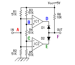 This circuit is the circuit which detects whether or not the change of the input voltage became above the band which was set. It makes the change which was detected with the infrared sensor have the non-sense width and it is the circuit to make the mis-detection little. It is the circuit to compare in the voltage but at the circuit this time, the operational amplifiers are used. 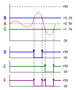 As for IC1, +3.3 V are applied to the positive input terminal as the reference voltage with the circuit of the upper limit voltage detection. If the voltage of the negative input terminal is less than +3.3 V, the output is the H level. When the voltage of the negative input terminal becomes more than +3.3 V, the output becomes the L level rapidly. As for IC1, +3.3 V are applied to the positive input terminal as the reference voltage with the circuit of the upper limit voltage detection. If the voltage of the negative input terminal is less than +3.3 V, the output is the H level. When the voltage of the negative input terminal becomes more than +3.3 V, the output becomes the L level rapidly.As for IC2, +1.7 V are applied to the negative input terminal as the reference voltage with the circuit of the minimum voltage detection. If the voltage of the positive input terminal is more than +1.7 V, the output is the H level. When the voltage of the positive input terminal becomes less than +1.7 V, the output becomes the L level rapidly. +2.5 V are applied to the negative input terminal of IC1 and the positive input terminal of IC2. And, the voltage changes when detecting the move of the person and so on with the infrared sensor. As for either of IC1 and IC2, when becoming the L level, the output becomes the L level. The diode which is put to the output of the IC is to prevent over-current's flowing from the other IC when either the IC becomes the L level.  The output of the window comparator is the pulse which is short because it becomes the L level only when the input crosses the upper limit or the minimum. It is difficult to work the relay of the output in this pulse. Therefore, it makes maintain the output using the 555 timer IC as the output circuit in the constant time. The output of the window comparator is the pulse which is short because it becomes the L level only when the input crosses the upper limit or the minimum. It is difficult to work the relay of the output in this pulse. Therefore, it makes maintain the output using the 555 timer IC as the output circuit in the constant time.The 555 timer begin the operation from the time when the trigger input (the A point) became the L level and maintain the output in the H level until it becomes the time which is decided with the capacitor (C) and the resistor (R). It continues the operation even if the input pulse returns to the H level when beginning the operation once. The time of the timer is possible to calculate by the following formula.
t = 1.1CR As for the operation of the 555 timer, refer to "555 timer". It is as follows when calculating at the value in the circuit this time.
The condition : C = 10µF, R = 100K-ohm
The operation of the timer continues for the about 1 second. Because this value changes with the error of the parts, it uses as the reference. If making R = 1M-ohm, in the operating time, it becomes the about 10 seconds. The circuit which connects with the reset terminal (the 4th pin) of the timer is the circuit which controls the operation of the output circuit in the light around. When the reset terminal is the H level, the timer is in the operation possible condition. It is the non-operating state when the reset terminal becomes the L level. In this case, it doesn't work even if the pulse enters the input. The Cds has the nature that the resistance value falls when the shining makes a hit and the resistance value becomes high when the shining is interrupted. In case of the condition that VR1 becomes the side of Cds, when the shining enters Cds, the reset terminal of the timer becomes the L level, the timer doesn't work. When the shining is interrupted, the reset terminal becomes the H level and the timer becomes the operation possible condition. In case of the condition that VR1 becomes the side of the power supply, irrespective of the resistance value of Cds, the reset terminal of the timer always becomes the H level, it is in the condition about which it is possible to work. The working light of the output circuit can be adjusted by the position of VR1. The diode which is connected with the output (the 3rd pin) and the reset terminal (the 4th pin) of the timer is to prevent from output's unjust operation. It maintains the reset terminal in the H level when the output becomes the H level. It is for the timer to work in the setup time even if the shining enters Cds on the way where the timer is working. The output of the timer is connected with the base of the transistor for the relay drive and when the B point becomes the H level, the transistor becomes the ON condition. The relay works with this and the output point of contact closes. The diode (D) to put to the coil of the relay is put to prevent from transistor's being broken at the voltage which occurs when the relay works. 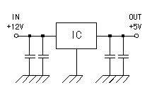 I am using +12 V as the input power supply. It is making +5 V to have used the 3 terminal regulator and to have been stable. The voltage of the inner circuit can be made higher, too, but the width with the detection voltage of the window comparator has spread when increasing the voltage simply. In the case, the resistor for the reference voltage setting by the comparator must be changed. |