[Menu]>[Manufacturing of Original PCB]


About the Printed Circuit Board


When making the circuit with the electronic parts of the resistors, the capacitors, the transistors, the ICs and so on, it is necessary to connect the lead line of each part appropriately. Also, each part must be fixed, too.
The printed circuit board is used to do the wiring among the parts and the fixation of the part.
The electronic circuits can be assembled even if it doesn't use the printed circuit board. It uses the wiring materials for the wiring and it should use the terminal board and so on for the fixation of the parts. Actually, the simple circuit sometimes assembles the printed circuit board without using it, too.
There are some advantages which use the printed circuit board.

Good one is made. Many sheet of the same circuits can be made with the same quality.
The same one is made whoever assembles.
Cheaply made.
(In the case for the industry)
If fixing (the soldering) in the parts even if it doesn't wire, the electronic circuits can be assembled.
It is possible to do the construction at short time and it can do the manufacturing cost cheaply.
All constructions can be mechanized, too.
Compactly made.The small wiring can be made using the print technique.


As the description up, the printed circuit board very suited the construction of the electronic circuits.

The printe circuit board is called the PCB or PWB(Printed Wiring Board). As well as Japan, to call the PCB is general.
In Japan, at first, it was called the PCB, but there is a pollution accident of another material(PolyChlorinated Biphenyls(PCB's) : it is the poison) in the 1960s and since it, we changed the name of the printed circuit board into the PWB.


The structure of the printed circuit board

The printed circuit board is doing the structure which stuck the wiring in the insulation board(Material such as the bakelite, the epoxy which doesn't transmit electricity) with the 1 to 2 mm thickness with the copper foil.
As for the thickness of the copper foil, the one of 30 to 40 µm is general.

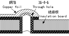
The copper foil is set up to the both sides of the insulation board and there is one which can picture the wiring pattern in the double sided, too.
In the industrial business, the through-hole is used to link the wiring of the both sides. This is the way of making a hole to connect the print pattern of the double sided electrically and then connecting the pattern of the double sided with the hole by the chemical copper plating.
When homemade, it is OK if making a small hole and letting through the copper wire and soldering on both sides.

Besides, the special equipment is necessary but there are various kind of printed circuit boards.
The one which has the shield(Earth plate to prevent the electromagnetic influence of the wiring of the double sided), inserting the sheet copper at the center of the insulation board.
The one to make the insulation board the multilayer structure and for the wiring pattern to become solid.(There are ones such as the 50 layers, too)
The one where the insulation board is thin like the film.


The printed circuit board making way outline

The copper foil in the wiring part doesn't stick the copper foil which did the form of the wiring. It dissolves the copper foil in the part (the insulated part) which is not the wiring in the way of being called the etching and it leaves only the wiring part.
Because it is, the printed circuit board before doing the etching uses that the copper foil is stuck in all surfaces of the insulation board.
To dissolve the copper foil in the unnecessary part is called the etching (Etching : being the corrosion copperplate art with the picture).
As the solvent to dissolve the copper, the solution of the Ferric Chloride is used.
The part to leave as the wiring masks (picturing the wiring pattern with the material which doesn't dissolve in the solution) beforehand so as not for the Ferric Chloride to melt it.
After doing the etching, peel off the mask. Then, paint the flux to prevent the corrosion of the copper.

When seeing the printed circuit board which is used with the electric product, the wiring surface is doing the green. This is because solder-resist is painted.
This is the one to prevent printed wiring's having solder. Of course, the printed wiring part which solderings the lead line of the part doesn't paint solder-resist.
When assembling the electronic circuits at the factory, it isn't soldered by the handwork and it does with the machine. It is the way of having soldered the wiring surface of the printed circuit board at once by soaking it in solder-sink (melted solder is stored).
At this time, it paints solder-resist to prevent solder's there being in the extra part.
solder-resist does the function to be painted for above-mentioned purpose and for it to prevent the corrosion of the wiring pattern, too.
It sometimes paints solder-resist in the purpose to prevent the corrosion of the wiring pattern when homemade, too.

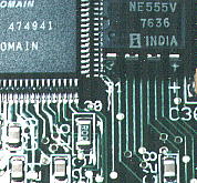
As for the recent parts, the SMT(Surface Mount Type) is used by the dwarfing. This doesn't soldering the lead line of the part in the back of the printed circuit board and solderings the lead line of the part to direct to wire.
In this case, in the industrial business, it doesn't use (it isn't possible to use) solder-sink and the cream solder is used. It paints the cream solder the soldering part of the printed wiring and it puts the part on it. It is the way of dissolving the cream solder in short time at high temperature and soldering it.
The quantity of the cream solder can be adjusted in detail and then in case of VLSI(Very Large Scale Integrated-circuit), there is not solder bridge(Condition which has been soldered with the lead line next) and high density soldering is made of this way.
As for the board of the personal computer and so on, this way is almost used.

To compare the printed wiring density, I attempted to put DIP-type IC(NE555).