Circuit explanation
of 4 Channel Adapter for the Oscilloscope
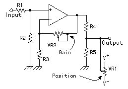 I used LM747 as the input amplifier. I used LM747 as the input amplifier.The power supply is ±12 V. Therefore, the maximum with the input voltage of the amplifier is to ±12 V. Because I want to make the permission value with the input voltage above it, I make the voltage of the input amplifier 1/10 with R1 and R2. When ±30 V are inputted, ±3 V are gained by the input terminal of the amplifier. The vertical position adjustment is making the direct current rise one above another with the output.(±5V) Because LM747 had the terminal for the offset control, I intended to use this. However, because the voltage change range was small, it wasn't possible to use for the justification. Originally, this terminal is not the terminal for the position adjustment. The way this time is the way that there is a little impossibility. When adjusting the position, the output voltage, too, has changed. It is possible to use if not making the top or bottom extremely. The signal vertical (the voltage axis) can be adjusted with VR1. But, that the oscilloscope to use can be displayed in the direct current is the condition. Because it wasn't possible to use the offset terminal, as the input amplifier, the operational amplifier can use TL084 with the housing of the four in the 1 package. Because pin connections are different, the pattern must be reformed. It is adjusting the mu factor of the amplifier with VR2. When VR2 is the smallest (the condition which connected the output of the amplifier and the negative input terminal), the mu factor of the amplifier becomes 1.(Noninverting Gain amplification) Because the circuit this time made R3=10K-ohm, VR2=250K-ohm, it is (1+VR2/R3)=26 times when maximizing VR2. Because it makes the input 1/10 by the resistance division, and 1/2 by R4 and R5. It doesn't become more than ±12 V . R4 and R5 are to drop the voltage of the output. This is because the IC for the switching which connects the output works by ±5 V. It breaks when connecting the output of the input amplifier directly. Because it is R4=15K-ohm, R5=10K-ohm, it is 10/(15+10)=1/2.5. When ±12 V are output from the input amplifier, the voltage which is gained by R5 becomes ±4.8 V. The way this time is not the way which is good because the noise occurs. When making the input signal 1/10, the output approaches the noise level. The amplifier has been amplified including the noise. 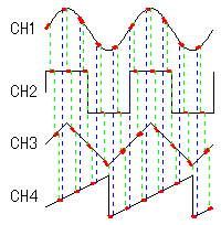 It is the circuit which does the switch of the four input signals. As the IC, it is using the thing for the switching of the analog signal. Because the power supply voltage of this IC is using ±5 V, it can handle the signal in the ±5 V range as the signal. According to the condition of the switch control line, the input signal of CH1-CH4 appears in the output. As for the figure on the left, the changing frequency is in the condition which isn't too fast to the frequency of the input signal. Because it is, the output signal (red) becomes the dotted line. Actually, if the input signal is lower sufficiently than the switching frequency, you can see the continued line. 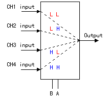 It uses the voltage of TTL(0V to +5V) to control the switching operation. The two control lines and the relation of the switching of the signal are as follows.
Only 0Y and 1Y can be connected with the output when making the control line B the L condition and the control line A the L or H as shown in the table . When not needing the 4 channels, it is like this. In case of the 2 channels, it is displayed at the duple density compared with the 4 channels.  It switches the analog switch using the pulse to have made oscillate with the spuare wave oscillator. It switches the analog switch using the pulse to have made oscillate with the spuare wave oscillator.In case of the 4 channels, the output of the oscillator is inputted to the flip-flop (FF) and makes twice of periods. The output of the FF connects with the input B of the analog switch. It connects the output of the oscillator with the input A directly. To make the 2 channels, it fixes the control line B of the analog switch on the L level. I used the two 2 input NAND gates to fix the control line B on the L level. n3 and n4 are to make the wave form sharp.
As for the NAND gate, as for some of the input, when becoming the L level, the H level is output irrespective of the condition of the other input. The change of the other input doesn't appear in the output. When the output of n1 is the H level, the output of n2 becomes the L level and the control line B of the analog switch is fixed on the L level. In this way, as for the control line of the analog switch, only A changes into the L and H and only CH1 and CH2 work. 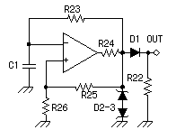 It is using the spuare wave oscillator to have made the operational amplifier with positive feedback. It is using the spuare wave oscillator to have made the operational amplifier with positive feedback.D2 and D3 are the 4.7-V Zener diode. It is the one to control the output voltage of the oscillator to about ±5 V. Also, D1 is the diode to be rectified for the output to become only the positive voltage. It is to adjust the output of the oscillator to TTL(0V to +5V). R24 is for the electric current to be prevented from flowing through D2 and D3 too much with the output of the operational amplifier. Because the frequency of the oscillator becomes the switching period of the analog switch, the frequency which is as high as possible is desirable for it. However, there is following problem.
Because it is the above, I make the oscillation frequency this time about 20 KHz. I used the operational amplifier with the good frequency characteristic to make the wave form sharp. It is as follows when comparing the standing-up time of the signal of usual operational amplifier (LM318) and LM6361 which was used this time.
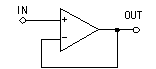 It uses the signal of CH1 as the external trigger signal of the oscilloscope. It uses the signal of CH1 as the external trigger signal of the oscilloscope.Be explaining the operation principle of the oscilloscope, to make display the stationary wave-form on the screen, it is necessary to make the period of the scan and the period of the input signal synchronize. The oscilloscope detects the standing-up or the standing falling of the observation signal inside and has the function to make the scan period synchronize automatically. However, when using this function, it has detected and it has scanned the standing-up or the standing falling by the switching at the period which is different from the input signal. Because it is, the input signal must be inputted as the external trigger signal. It uses the signal of CH1 as the external trigger signal through the amplifier with the mu factor 1. 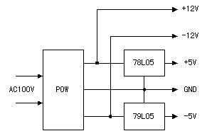 The ±12 V power supply is necessary for the operational amplifier to work. Also, it uses ±5 V as the power supply with the analog switch and it uses +5 V as the power supply of the logic circuit. First, it makes the DC ±12 V voltage from AC100 V and it makes the stable ±5V voltage with three terminal regulators. The circuit this time doesn't need the big power supply with the current-carrying capacity. Because it was, I used the small switching power supply and 3 terminal regulators. |
||||||||||||||||||||||||||||||||||||||||||||||||