8bits Latch Register
|
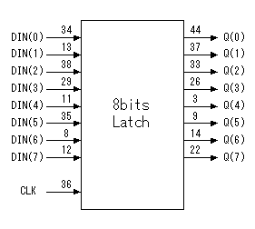
On this page, I will introduce the 8 bits Latch Register.
The latch register is the storage circuit to maintain data. Concretely, it maintains data by the rising edge of the clock pulse. Input data in case of this timing is taken in to the register. Even if the input data changes, the output doesn't change until the rising edge of the next clock pulse occurs. In the logic this time, I made maintain data with byte(8bits). However, you can make the register of the needed bits if you change logic. Pin lock isn't specified. As the device, it deals with CPLD(XC9536-PC44).
Operating state table
|