|
There are several kinds of development language( HDL:Hardware Description Language ) to design CPLD.
ABEL-HDL, VerilogHDL, VHDL are typical languages.
In the software of WebPACK, either of these languages can be used.
I decided to use VHDL.
The comparative easiness of the description and it seems to be the present mainstream.
The full spelling of VHDL is "Very high speed integrated circuit Hardware Description Language".
The language specification to introduce on this page is a part only in VHDL.
The details see a professional book.
Below, I will explain the basic syntax of VHDL.
Actually, it is more complicated and it is profound. This is just a guide.
In the explanation, the description for Xilinx Project Navigator is contained.
So, there is possibility that the description which is different from the other tool is contained.
 Basic Syntax of VHDL Basic Syntax of VHDL
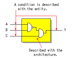
 Entity and Architecture Entity and Architecture
When circuit composition is described in VHDL, the concept of the entity and the architecture is used.
In the entity, the input condition of the circuit block to design(Port declaration) and the parameter with bit length and so on(Generic declaration) are defined.
In the architecture, the logical structure of the circuit block to design is described.
The Basic Syntax
 |
library ieee;
use ieee.std_logic_1164.all;

entity (entity name) is

(entity statements)

end (entity name);

architecture (architecture name) of (entity name) is
begin

(architecture statements
end (architecture name); |
|
The blue part of the character shows the character of the format which is prescribed in VHDL.
There is not a distinction of the uppercase, the lowercase.
The Comment
All character after continuing two hyphens (--) becomes a comment. A comment isn't related with the processing.
The comment is effective only in 1 line. To make the following line a comment, (--) must be put to the head.
library ieee;  -- Declaration of library
-- comment |  | The red part is a comment. |
Library declaration
In Library, the various definition group to use in VHDL is declared.
Generally, the declaration of the standard logic which is prescribed in the IEEE is specified.
There is various declaration but it seems OK if declaring the following 2 lines.
library ieee;
use ieee.std_logic_1164.all; |
The above declares all definitions which are prescribed in STD_LOGIC_1164 of the IEEE.
When using Xilinx Project Navigator, these declare statements are already written when making a source file newly.
When you design the more complicated circuit, more declaration must be done.
When using an arithmetic operation in the processing, STD_LOGIC_UNSIGNED must be specified.
use ieee.std_logic_unsigned.all;
Entity statements
In Entity, a port declaration, an attribute declaration, a generic declaration and so on are written.
When Entity ends, it writes END. The entity name behind end can be omitted.
Below, I will explain a port declaration and an attribute declaration.
 Port declaration Port declaration
All input/output ports are specified by the Port declaration.
Syntax
port (port name:directiondata type name;
port name:directiondata type name; (port name:directiondata type name;
port name:directiondata type name;
 port name:directiondata type name);
 |
 :space :space
If the direction, the data type are the same, it is possible to join the port name by dividing in comma (,).
In above-mentioned syntax, the new line is started after semicolon (;) for that it is easy to see. However, it may write in the same line.
The following five kinds can be specified as the direction.
| in | Input port |
| out | Output port |
| inout | Input/Output both port |
| buffer | Output (It is possible to reuse inside). |
| linkage | It is possible to bind in any direction. |
Generally, in or out is used.
A logic type is specified by the type name.
Generally, std_logic or std_logic_vector is used. Vector is used when making more than one piece of the same logic.
To specify a type, "ieee.std_logic_1164.all" must be specified by Library. |
Ex. 1
|  | port (
a,b,c : in std_logic;
y : out std_logic); |
a, b and c are the input ports of the standard logic.
y is the output port of the standard logic. |
|  | port (
a,b : in std_logic_vector(2 downto 0);
y : out std_logic_vector(2 downto 0)); |
| a, b and c have the set from 0 to 2 respectively. |
Attribute declaration
There are lot of kinds of attribute which can be used in Xilinx Project Navigator.
attribute PIN_ASSIGN of object : object_type is "pin_name";
attribute LOC of object_list : object_type is "function_block_name";
attribute KEEP of object_list : object_type is "TRUE";
attribute DONT_OPTIMIZE of object_list : object_type is "TRUE";
attribute FAST | SLOW of object_list : object_type is "TRUE";
attribute BUFG of object_list : object_type is "CLK" | "OE" | "SR";
attribute INIT of object_list : object_type is "S" | "R";
attribute PWR_MODE of object_list : object_type is "LOW" | "STD";
attribute REG of object_list : object_type is "CE" | "TFF";
attribute TNM of object_list : object_type is "string";
Before using these attribute declarations, it is necessary to declare always below.
attribute attribute_name : string;
I will show the attribute declaration example of the pin assignment below.
The port name(object) must be specified by the port declaration beforehand.
Ex. The example which assigned the A, B, Y ports to 1, 2, 3 pins respectively.
| 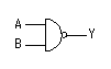 | library ieee;
use ieee.std_logic_1164.all;
entity Ex1 is
port( A : in std_logic;
B : in std_logic;
Y : out std_logic);
attribute pin_assign : string;
attribute pin_assign of A : signal is "1";
attribute pin_assign of B : signal is "2";
attribute pin_assign of Y : signal is "3";
end;
architecture SAMPLE of Ex1 is
begin
Y <= A nand B;
end SAMPLE; |
The pin assignment by the fitting result
      T  T  T           T  T  T  V  T
      I  I  I           I  I  I  C  I
      E  E  E  y  b  a  E  E  E  C  E
      --------------------------------
     /6  5  4  3  2  1  44 43 42 41 40 \
TIE | 7                             39 | TIE
TIE | 8                             38 | TIE
TIE | 9                             37 | TIE
GND | 10                            36 | TIE
TIE | 11         XC9536-5-PC44      35 | TIE
TIE | 12                            34 | TIE
TIE | 13                            33 | TIE
TIE | 14                            32 | VCC
TDI | 15                            31 | GND
TMS | 16                            30 | TDO
TCK | 17                            29 | TIE
    \ 18 19 20 21 22 23 24 25 26 27 28 /
      --------------------------------
      T  T  T  V  T  G  T  T  T  T  T
      I  I  I  C  I  N  I  I  I  I  I
E E E C E D E E E E E |
When doing "Lock Pins" using Xilinx Project Navigator, pin assignment is recorded to the UCF file. So, to change pin assignment after"LockPins", the record data must be changed using "Edit UCF file" in the "Processes for Current Source" window.
Architecture statements
In Architecture, the logic of the circuit is written.This part is the main CPLD design part.
As for this description, there are a lot of rules. Here, it isn't possible to write completely.
I will mention only a basic part below.
Syntax
architecture(architecture name)of(entity name)is

   <declare statements>

begin

   <processing statements>

end(architecture name) |
:space
The architecture name behind end can be omitted.
Declare statements
In the declare statements, signal declaration, component declaration and so on are written.
I will introduce signal declaration below.
Signal declaration
In the signal declaration, the signal to use inside is defined.
Ex.
| 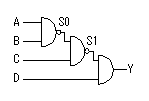 | library ieee;
use ieee.std_logic_1164.all;
entity Ex2 is
port( A : in std_logic;
B : in std_logic;
C : in std_logic;
D : in std_logic;
Y : out std_logic);
end;
architecture SAMPLE of Ex2 is
signal S0,S1 : std_logic;
begin
S0 <= A nand B;
S1 <= S0 nand C;
Y <= S1 and D;
end SAMPLE; |
S0 and S1 are the signal to use only in the logic inside.
A data type is specified like the port declaration by the signal declaration. |
Processing statements
In the processing statements, following processing sentences can be written.
Concurrent
sentences |
In the concurrent sentences, the independent logic processing sentences are written.
S0 <= A and B
Y <= S0 nand D
Above-mentioned sentences are independently processed respectively.
It is the same even if it writes the line of S0 and the line of Y oppositely.
It is called concurrent sentence because it seems to be processing at the same time irrespective of the order to write. |
Process
sentences |
In the process sentences, described sentences are processed in the order from top.
In the sentence, the conditional statements of "IF" and "CASE" can be described. |
Syntax of the process sentence
process(input port name)

begin

  < sequential statements >

endprocess; |
:space
Below, I will explain "IF sentence" and "CASE sentence" to use in the process sentence.
"IF" sentence
Syntax
(1)
if (condition) then
  <sequential statements>
end if; |
|
(2)
if (condition) then
  <sequential statements>
else
  <sequential statements>
end if; |
|
(3)
if (condition) then
  <sequential statements>
elsif (condition) then
    <sequential statements>
else
    <sequential statements>
end if; |
|
|
"CASE" sentence
Syntax
case (condition) is
  when "condition 1" => port name <= "value 1";
  when "condition 2" => port name <= "value 2";


  when "condition n" => port name <= "value n";
  when others => port name <= "value x";
end case; |
|
3 to 8 Demultiplexer ( same as 74138 )
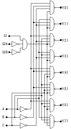 | The pin assignment by the fitting result
                                    y
      T  T  T           T  T  T  V  <
      I  I  I           I  I  I  C  0
      E  E  E  c  b  a  E  E  E  C  >
      --------------------------------
     /6  5  4  3  2  1  44 43 42 41 40 \
 g1 | 7                             39 | y<1>
g2a | 8                             38 | y<2>
g2b | 9                             37 | y<3>
GND | 10                            36 | y<4>
TIE | 11         XC9536-5-PC44      35 | y<5>
TIE | 12                            34 | y<6>
TIE | 13                            33 | y<7>
TIE | 14                            32 | VCC
TDI | 15                            31 | GND
TMS | 16                            30 | TDO
TCK | 17                            29 | TIE
    \ 18 19 20 21 22 23 24 25 26 27 28 /
      --------------------------------
      T  T  T  V  T  G  T  T  T  T  T
      I  I  I  C  I  N  I  I  I  I  I
E E E C E D E E E E E |
001
002
003
004
005
006
007
008
009
010
011
012
013
014
015
016
017
018
019
020
021
022
023
024
025
026
027
028
029
030
031
032
033
034
035
036
037
038
039 | library ieee;
use ieee.std_logic_1164.all;
entity DECODER1 is
port ( A,B,C,G1,G2A,G2B : in std_logic; -- INPUT and OUTPUT declaration
Y : out std_logic_vector(7 downto 0));
attribute pin_assign : string; -- Pin assign
attribute pin_assign of A : signal is "1";
attribute pin_assign of B : signal is "2";
attribute pin_assign of C : signal is "3";
attribute pin_assign of G1 : signal is "7";
attribute pin_assign of G2A : signal is "8";
attribute pin_assign of G2B : signal is "9";
attribute pin_assign of
Y : signal is "33,34,35,36,37,38,39,40";
end DECODER1;
architecture SAMPLE of DECODER1 is
signal IN_DATA : std_logic_vector(2 downto 0); -- Internal signal declaration
begin
IN_DATA <= C & B & A; -- Binding vector
process( IN_DATA, G1, G2A, G2B ) begin
if( G1='1' and G2A='0' and G2B='0' ) then -- Judgement of gate condition
case IN_DATA is -- Judgement of input data
when "000" => Y <= "11111110";
when "001" => Y <= "11111101";
when "010" => Y <= "11111011";
when "011" => Y <= "11110111";
when "100" => Y <= "11101111";
when "101" => Y <= "11011111";
when "110" => Y <= "10111111";
when "111" => Y <= "01111111";
when others => Y <= "XXXXXXXX"; -- Illegal condition
end case;
else
Y <= "11111111"; -- Gate OFF condition
end if;
end process;
end SAMPLE; |
|
The above is the decoder circuit which changes the binary input of 3 bits into eight pieces of output.
It has the function which is the same as 74138 (Decoder IC).
If you make only this function, it had better use 74138. I made this logic for the practice.
I will explain some points for this description below.
| Line | Comment |
| 006 |
Eight vectors are used for output (Y).
"Downto" is used because it makes descending order(7->6->5->4->3->2->1->0) in the specification this time.
"To" can be used to make a ascending order(0->1->2->3->4->5->6->7).
In the case, the order of all arrangements must be reconsidered. |
| 015 | Y is specified in eight pieces of assignment of the pin because it is vector. |
| 019 |
A signal for the logic judgment inside is defined.
It is made three vectors because it is 3 bits. |
| 021 | The inputs are connected with the inner signal. Because the input is 1 bit respectively, they are binded using &. |
| 022 | The input signal of the process sentence is specified. They are 3-bit IN_DATA and the gate input (G1,G2A,G2B). |
| 023 | When all conditions of the gate are '1', the logic as it becomes the process after 023 is created. |
024
-034 | The logic which sets a condition to output (Y) by the condition of IN_DATA is created. |
| 035 | Logic in case of one of the gate conditions is '0' is created. |
| 036 | The logic which makes all output (Y) to '1' is created. |
|