|
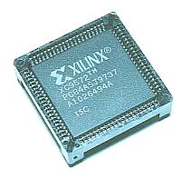
The following item is used to know the position of the pin.
*The direction of the printed name.
*A corner in the upper left is shaved.
A pin numbering is counterclockwise given from the center of the line in the topside. Note is necessary to the pin arrangement by the Function Block and the macrocell because it a little irregular-ly. In case of XC9572-PC84, the macrocells which corresponds to the input/output pins are 69 macrocells in the 72 macrocells. In case of XC95108-PC84, they are 69 macrocells in the 108 macrocells.
The macrocells which don't correspond to the input/output pins can be used only in the logic circuits inside.
The figure below is the top view of CPLD of 84 pins.
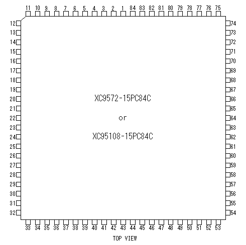 The pins colored purple are pins for JTAG.
Pin Diagram of XC9572-15PC84C
The pins colored purple are pins for JTAG.
Pin Diagram of XC9572-15PC84C
FB : Function Block number
| Pin number | FB | Macrocell |  | Pin number | FB | Macrocell |
| 1 | 1 | 2 | 43 | 3 | 13 |
| 2 | 1 | 5 | 44 | 4 | 2 |
| 3 | 1 | 6 | 45 | 3 | 16 |
| 4 | 1 | 1 | 46 | 4 | 1 |
| 5 | 1 | 8 | 47 | 4 | 5 |
| 6 | 1 | 3 | 48 | 4 | 8 |
| 7 | 1 | 4 | 49 | GND |
| 8 | GND | 50 | 4 | 9 |
| 9 | 1 | 9 | 51 | 4 | 3 |
| GCK1 |
| 10 | 1 | 11 | 52 | 4 | 4 |
| GCK2 |
| 11 | 1 | 7 | 53 | 4 | 11 |
| 12 | 1 | 14 | 54 | 4 | 6 |
| GCK3 |
| 13 | 1 | 10 | 55 | 4 | 7 |
| 14 | 1 | 15 | 56 | 4 | 14 |
| 15 | 1 | 17 | 57 | 4 | 10 |
| 16 | GND | 58 | 4 | 12 |
| 17 | 3 | 2 | 59 | TDO |
| 18 | 1 | 12 | 60 | GND |
| 19 | 3 | 5 | 61 | 4 | 13 |
| 20 | 1 | 13 | 62 | 4 | 16 |
| 21 | 3 | 8 | 63 | 2 | 1 |
| 22 | VccIO 3.3V/5V | 64 | VccIO 3.3V/5V |
| 23 | 1 | 16 | 65 | 4 | 15 |
| 24 | 1 | 18 | 66 | 4 | 17 |
| 25 | 3 | 1 | 67 | 2 | 3 |
| 26 | 3 | 9 | 68 | 2 | 4 |
| 27 | GND | 69 | 2 | 2 |
| 28 | TDI | 70 | 2 | 5 |
| 29 | TMS | 71 | 2 | 6 |
| 30 | TCK | 72 | 2 | 8 |
| 31 | 3 | 3 | 73 | VccINT 5V |
| 32 | 3 | 4 | 74 | 2 | 9 |
| GSR |
| 33 | 3 | 11 | 75 | 2 | 10 |
| 34 | 3 | 6 | 76 | 2 | 7 |
| GTS1 |
| 35 | 3 | 7 | 77 | 2 | 11 |
| GTS2 |
| 36 | 3 | 14 | 78 | VccINT 5V |
| 37 | 3 | 15 | 79 | 2 | 12 |
| 38 | VccINT 5V | 80 | 2 | 13 |
| 39 | 3 | 17 | 81 | 2 | 14 |
| 40 | 3 | 10 | 82 | 2 | 16 |
| 41 | 3 | 12 | 83 | 2 | 15 |
| 42 | GND | 84 | 2 | 17 |
|
Pin Diagram of XC95108-15PC84C
FB : Function Block number
| Pin number | FB | Macrocell | | Pin number | FB | Macrocell |
| 1 | 1 | 2 | 43 | 5 | 15 |
| 2 | 1 | 3 | 44 | 5 | 17 |
| 3 | 1 | 5 | 45 | 6 | 2 |
| 4 | 1 | 6 | 46 | 6 | 3 |
| 5 | 1 | 8 | 47 | 6 | 5 |
| 6 | 1 | 9 | 48 | 6 | 6 |
| 7 | 1 | 11 | 49 | GND |
| 8 | GND | 50 | 6 | 8 |
| 9 | 1 | 12 | 51 | 6 | 9 |
| GCK1 |
| 10 | 1 | 14 | 52 | 6 | 11 |
| GCK2 |
| 11 | 1 | 15 | 53 | 6 | 12 |
| 12 | 1 | 16 | 54 | 6 | 14 |
| GCK3 |
| 13 | 1 | 17 | 55 | 6 | 15 |
| 14 | 3 | 2 | 56 | 6 | 17 |
| 15 | 3 | 3 | 57 | 4 | 2 |
| 16 | GND | 58 | 4 | 3 |
| 17 | 3 | 5 | 59 | TDO |
| 18 | 3 | 6 | 60 | GND |
| 19 | 3 | 8 | 61 | 4 | 5 |
| 20 | 3 | 9 | 62 | 4 | 6 |
| 21 | 3 | 11 | 63 | 4 | 8 |
| 22 | VccIO 3.3V/5V | 64 | VccIO 3.3V/5V |
| 23 | 3 | 12 | 65 | 4 | 9 |
| 24 | 3 | 14 | 66 | 4 | 11 |
| 25 | 3 | 15 | 67 | 4 | 12 |
| 26 | 3 | 16 | 68 | 4 | 14 |
| 27 | GND | 69 | 4 | 15 |
| 28 | TDI | 70 | 4 | 17 |
| 29 | TMS | 71 | 2 | 2 |
| 30 | TCK | 72 | 2 | 3 |
| 31 | 3 | 17 | 73 | VccINT 5V |
| 32 | 5 | 2 | 74 | 2 | 5 |
| GSR |
| 33 | 5 | 3 | 75 | 2 | 6 |
| 34 | 5 | 5 | 76 | 2 | 8 |
| GTS1 |
| 35 | 5 | 6 | 77 | 2 | 9 |
| GTS2 |
| 36 | 5 | 8 | 78 | VccINT 5V |
| 37 | 5 | 9 | 79 | 2 | 11 |
| 38 | VccINT 5V | 80 | 2 | 12 |
| 39 | 5 | 11 | 81 | 2 | 14 |
| 40 | 5 | 12 | 82 | 2 | 15 |
| 41 | 5 | 14 | 83 | 2 | 16 |
| 42 | GND | 84 | 2 | 17 |
|
|