[Menu]>[Electronic circuit beans collection]>[555 oscillator]


Circuit explanation for 555 oscillator


Block diagram

NE555 is composed of the voltage comparators, the flip-flop and the transistor for the discharge. The composition is simple, but it is excellent one.
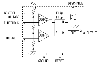
Three resistors are connected with the inside in series and the power supply voltage(Vcc) is divided in 3. This composition is an excellent point. 1/3 with power supply voltage is applied to the positive input terminal of the comparator (COMP1) and the voltage of 2/3 is applied to the negative terminal of the comparator (COMP2). When the voltage of the trigger terminal(TRIGGER) is less than 1/3 of the power supply voltage, the S terminal of the flip-flop(FF) becomes H level and an FF is set. When the voltage of the threshold terminal(THRESHOLD) is more than 2/3 of the power supply voltage, the R terminal of the FF becomes H level and an FF is reset.


The oscillation operation explanation
    I will explain the circuit operation below.

The condition immediately after the turning on


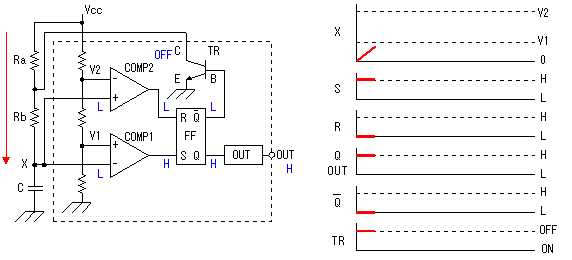
Immediately after a power supply voltage is supplied, as for the FF, the Q becomes H and becomes L condition. Because is the L, TR is in the OFF condition and the electric current flows through the resistor of Ra and the Rb at the capacitor (C). Immediately after a power supply voltage is supplied, the electric charge isn't stagnant in capacitor(C). So the voltage of the X point starts from 0V. Because the X point is lower than V1 of COMP1, the S terminal of the FF becomes the H condition. With this, the Q becomes H, becomes L condition but they are in the condition already. On the other hand, because the COMP2 (+) terminal is lower than V2, the output of COMP2 becomes the L and the FF is stable in this condition.


Output's reverse (1)


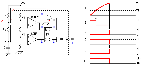
When the voltage of the X point crosses V1 of COMP1, the output of COMP1 becomes L. However, this change doesn't change the condition of the FF. The output of COMP2 becomes the H condition when the voltage of the X point rises more and reaches V2 of COMP2. With this, the R terminal of the FF becomes H and the output state of the FF reverses. The Q becomes the L condition and becomes the H condition. At this time, OUT changes into the L from H. Because became the H condition, TR becomes the ON condition. Because the interface of Ra and the Rb becomes the grounded condition, the electric current which was flowing through C so far through Ra and the Rb gets not to flow through capacitor(C). The electric charge which was stagnant in capacitor(C) begins the discharge through the Rb and TR. Voltage of the X point begins to go down with this discharge. Because voltage of the X point goes down, the voltage of the COMP2 (+) terminal becomes less than V2 and the R terminal of the FF changes into the L condition from H. This change doesn't change the condition of the FF.
It is only in a little time that the R terminal of the FF becomes the H condition.


Output's reverse (2)


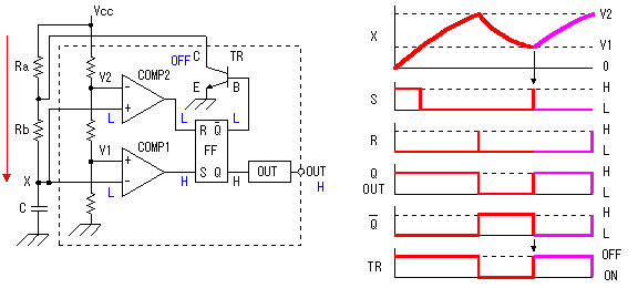
Because TR becomes ON, as for the electric charge of capacitor(C), it continues the discharge and the voltage of the X point falls. When the voltage of the X point becomes equal to or less than V1 of COMP1, the output of COMP1 becomes the H condition and the S terminal of the FF becomes the H condition. This changes the Q of the FF to H and changes into the L condition. Because became the L condition, TR becomes the OFF condition and the discharge from capacitor(C) stops. The electric current flows through Ra and the Rb again in capacitor(C) and the electric charge begins to store up. When the electric charge begins to store up in capacitor(C), voltage of the X point begins to go up and the output of COMP1 becomes the L condition immediately. After that, it repeats this operation and the signal of the square wave is output.

When charging (accumulating the electric charge) capacitor(C), the electric current flows through Ra and the Rb and in case of the discharge (missing the electric charge), it passes only the Rb. So, the time of the charging and the time of the discharge are different. By making the Rb compared with Ra big, the difference of both becomes small but can not make the same at all. To make the same, it is good if Ra is 0 ohm, but in the case, Vcc is directly connected with TR and TR has broken. Don't make Ra = 0 ohm absolutely. If doing the ratio of Ra and the Rb by several times, in case of the practical use, there is not a problem.