Operation explanation
of the square wave oscillator (2)
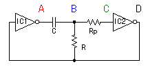 The circuit diagram of the oscillation circuit is written like the circuit to have posted on the page at the head. However, I wrote like the left figure for the circuit to be easy to understand. When seeing this circuit diagram, you find that it is composed of the differentiation circuit by the capacitor (C) and the resistor (R). The differentiated wave appears in the B point when the square wave is applied to the A point. This differentiated wave isn't mathematical. It becomes the diagonal straight line when differentiating the square wave mathematically. However, the output of this circuit is the curve. As for the differentiation circuit by the CR, refer to "Differentiation circuit". 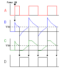 Immediately after turning on, the output of IC1 and IC2 becomes either of the H level or the L level. In this explanation, I assume that the output of IC1 is the H level and the output of IC2 is the L level. When the output of IC1 (the A point) becomes the H level, the B point becomes the same voltage as A point at first. However, as the electric charge stores up at the capacitor (C), the voltage of the B point goes down. This falling rate is decided by the value of the capacitor (C) and the resistor (R). The VTH on the graph of the B point shows the threshold voltage of IC2. The input of IC2 is judged to be the H level when the voltage of the B point is higher than VTH and the output of IC2 becomes the L level. Oppositely, the input of IC2 is judged to be the L level when the voltage of the B point is lower than VTH and the output of IC2 becomes the H level. So, the output of IC2 (the D point) becomes the L level while the B point is higher than VTH. The input of IC2 is judged to be the L level when the charging (the electric charge is stored up) to the capacitor (C) progresses and the voltage of the B point becomes VTH. Then, the output of IC2 (the D point) changes into the H level rapidly. When the D point changes into the H level, the output of IC1 (the A point) changes into the L level from the H level. That is, the polarity with the input voltage of the differentiation circuit of C and R becomes opposite. The electric charge is stored up by the previous operation at the capacitor (C). The voltage of the both edges of the capacitor (C) becomes the voltage to have subtracted the threshold voltage (VTH) from the power supply voltage (VDD). When the reverse voltage is applied to the CR circuit in this condition, the voltage of the B point becomes the -(negative) threshold voltage (-VTH). After that, the electric charge which is opposite is stored up to the capacitor (C) and the voltage of the B point rises gradually. When the B point becomes the VTH, the input of IC2 is judged to be the H level and the output of IC2 (the D point) becomes the L level. With it, the output of IC1 (the A point) becomes the H level. In this case, the voltage of the B point becomes the voltage to have added the power supply voltage (VDD) and the threshold voltage (VTH). The oscillation is done by repeating above operation. The resistor Rp is put in the purpose to prevent excessive electric current's flowing through the input of IC2. As the explanation above, the voltage which is higher than the power supply voltage or the voltage which is lower than 0 V appears in the B point. This is the resistor for IC2 not to break by this voltage. The circuit which protects the IC from the extraordinary input voltage is prepared for the inner circuit of the CMOS. This circuit is making bypass the electric current when the abnormal voltage is applied to the input with the circuit by the diodes. However, when the excessive electric current flows, this protection network breaks too. Then, the IC breaks. In case of the CMOS, because the input electric current is small, the resistor as much as tens of K-ohm to 100K-ohm is used. The value of this resistor isn't related with the oscillation frequency. |