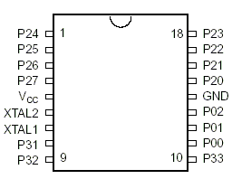
Pin #
Symbol
Function
Direction

Pin 7=STOP mode recovery
R247 = R3M.D0 (PP/OC)
Pin # |
Symbol |
Addr | Function |
Mode | Direction |
 |
|---|---|---|---|---|---|---|
| 1–4 | P24–P27 | R2 | Port 2 Pins 4,5,6,7 Pin 7=STOP mode recovery |
R246 = P2M (In/Out) R247 = R3M.D0 (PP/OC) |
Bidirectional | |
| 5 | VCC | Power Supply to 7v | Source | |||
| 6 | XTAL2 | Crystal Osc. | Clock Output | |||
| 7 | XTAL1 | Crystal Osc. | Clock Input | |||
| 8 | P31 | R3 | Port 3 Pin 1 or AN1. TIN, IRQ2 | R247 = P3M.D1 (AN/DG) | Input | |
| 9 | P32 | R3 | Port 3 Pin 2 or AN2. IRQ0, /IRQ3 | Input | ||
| 10 | P33 | R3 | Port 3 Pin 3 or AN REF. IRQ1 | Input | ||
| 11–13 | P00–P02 | R0 | Port 0 Pins 0,1,2 | R248 = P01M.D0 (In/Out) | In/Output | |
| 14 | GND | Ground | Sink | |||
| 15–18 | P20–P23 | R2 | Port 2 Pins 0,1,2,3 | R246 = P2M (In/Out) | In/Output |
IO Drive ability: Any single IO pin can source or sink 25mA, a single port can source 45mA or sink 60mA. Total power is 1.65 W, sourcing 220mA and sinking 300mA Ports 1 and 2 (not 3) can take Vss-0.7 to Vss+12 volts.
Power consumption: At 2, 8 and 12 MHz, respectivly, base current draw will be less than 11, 15 or 20 mA while running (no IO drive) and 5, 6, and 7 mA in standby (HALT). When stopped, with WDT not running and all inputs at Vcc or Vss, analog inputs at Vcc if enabled, current draw will be less than 20uA with 1uA typical. This is for the standard temperature range parts.
P0: 3-bit, input (P01M=00h) or output port (P01M=01h), Schmitt triggered, CMOS-compatible. Auto Latch puts valid CMOS levels on all pins when not otherwise driven.
P2: 8-bit, bidirectional (P2M.D0-7, Out=0, In=1), Schmitt-triggered, CMOS-compatible. The port as a whole can be set, via P3M.D0, so that any outputs are open drain (D0=0) or push-pull (D0=1). Auto Latch puts valid CMOS levels on all pins when not otherwise driven.
P3: 3-bit, input only, Schmitt-triggered, CMOS-compatible, (when P3M.D1=0) or Analog inputs comparing P31 with P33 at P3.1, and P32 with P33 at P3.2 (P3.3 is tied hi in analog mode) (when P3M.D1=1). In either case, the results feed IRQ0-2 (Falling Edge), IRQ3 (Rising Edge), and the input for Timer 1.
The timers have a Range of 1-256 Decimal 01-00 HEX. Loading a timer with 0 results in a count of 256.
T0: Source from main clock, 6 bit programmable prescaler (PRE0.D2-7), 8 bit programmable (T0 Write) counter (T0 Read). Can be disabled (TMR.D1=0) or reloaded (TMR.D0=1) programatically. Stop at zero (PRE0.D0=0) or reload inital value (PRE0.D0=1) for Modulo N operation. IRQ4 at end of count.
T1: Source is Clock/4 (PRE1.D1=1) or P31 (PRE1.D1=0), 6 bit programmable prescaler (PRE1.D2-7), 8 bit programmable (T1 Write) counter (T1 Read). Can be disabled (TMR.D3=0) or reloaded (TMR.D2=1) programatically. Stop at zero (PRE1.D0=0) or reload inital value (PRE1.D0=1) for Modulo N operation. Use P31 as clock (TMR.D4-5=00), retriggerable (TMR.D4-5=11) or non-retriggerable (TMR.D4-5=10) start trigger, or a gate input for the internal clock(TMR.D4-5=01). IRQ5 at end of count.
Ideal for a minimal controller
See also:
LD RP, #%0F 		;select Bank F
LD %0B, #00110100B 	;selects P27 as the Stop-
			;Mode Recovery pin.
This code must be removed before final ROM code submission or OTP programming. Note that P27 must be in Input Mode, which is accomplished with the following code:
LD P2M, #1xxxxxxxB
NOP 			;clears pipeline
Stop 			;halts processor
| file: /Techref/zilog/Z86E0812PEC.htm, 8KB, , updated: 2008/8/29 19:53, local time: 2025/10/14 00:51,
216.73.216.53,10-2-207-162:LOG IN
|
| ©2025 These pages are served without commercial sponsorship. (No popup ads, etc...).Bandwidth abuse increases hosting cost forcing sponsorship or shutdown. This server aggressively defends against automated copying for any reason including offline viewing, duplication, etc... Please respect this requirement and DO NOT RIP THIS SITE. Questions? <A HREF="http://techref.massmind.org/Techref/zilog/Z86E0812PEC.htm"> Zilog Z86E0812PEC, Embedded microcontroller</A> |
| Did you find what you needed? |
Welcome to massmind.org! |
Welcome to techref.massmind.org! |
.